

76
P. Kumar et al.
Nevertheless, the penetration depth of μRS in the backscatter configuration is still
very small and hence this method can be used to obtain stress information from near
surface regions only. As shown in Fig. 4.3b, the stress in Si around a TSV strongly
depends on the distance from the via-end: at very near the surface (as measured
using short wavelength laser), the stress becomes less tensile away from the via
end, whereas at slightly below depth (as measured using long wavelength laser), the
stress transitions from being compressive to tensile as one moves away from the via
end. Since the stress-state in the Si wafer is generally tri-axial, it is challenging to
measure all stress-components via Raman spectroscopy. Nevertheless, by combining
with FEA, μRS has been utilized to yield good estimates of the three-dimensional
stress state in the wafer [23–25]. It should be noted that metals are not Raman-active
and therefore the stress state of Cu cannot be measured using this technique and has
to be derived indirectly from measurements on Si.
4.2.2.3 X-Ray Diffraction (XRD) Based Techniques
To directly measure the localized strain, and hence the stress-field in Cu TSVs, X-ray
diffraction, used in conjunction with a cross-section TEM or a synchrotron radiation
source, may be used to determine stress-induced changes in unit cell parameter
from the equilibrium [26–28]. This can also be used to measure stress in Si nondestructively with very high resolution. Although XRD typically yields only average
stress values, by focusing high energy X-rays in a synchrotron to a small beam
size and rastering it on the sample, full strain and stress tensors from submicrometer
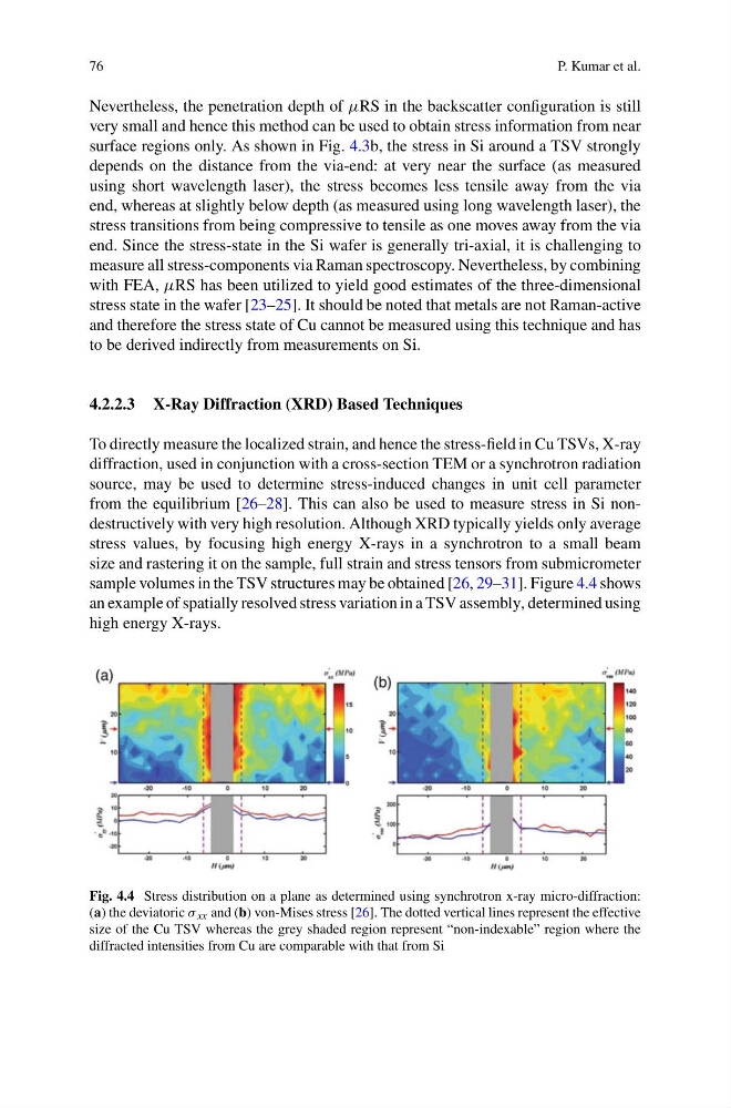
sample volumes in the TSV structures may be obtained [26, 29–31]. Figure 4.4 shows
an example of spatially resolved stress variation in a TSV assembly, determined using
high energy X-rays.
Fig. 4.4 Stress distribution on a plane as determined using synchrotron x-ray micro-diffraction:
(a) the deviatoric σ xx and (b) von-Mises stress [26]. The dotted vertical lines represent the effective
size of the Cu TSV whereas the grey shaded region represent “non-indexable” region where the
diffracted intensities from Cu are comparable with that from Si
P. Kumar et al.
Nevertheless, the penetration depth of μRS in the backscatter configuration is still
very small and hence this method can be used to obtain stress information from near
surface regions only. As shown in Fig. 4.3b, the stress in Si around a TSV strongly
depends on the distance from the via-end: at very near the surface (as measured
using short wavelength laser), the stress becomes less tensile away from the via
end, whereas at slightly below depth (as measured using long wavelength laser), the
stress transitions from being compressive to tensile as one moves away from the via
end. Since the stress-state in the Si wafer is generally tri-axial, it is challenging to
measure all stress-components via Raman spectroscopy. Nevertheless, by combining
with FEA, μRS has been utilized to yield good estimates of the three-dimensional
stress state in the wafer [23–25]. It should be noted that metals are not Raman-active
and therefore the stress state of Cu cannot be measured using this technique and has
to be derived indirectly from measurements on Si.
4.2.2.3 X-Ray Diffraction (XRD) Based Techniques
To directly measure the localized strain, and hence the stress-field in Cu TSVs, X-ray
diffraction, used in conjunction with a cross-section TEM or a synchrotron radiation
source, may be used to determine stress-induced changes in unit cell parameter
from the equilibrium [26–28]. This can also be used to measure stress in Si nondestructively with very high resolution. Although XRD typically yields only average
stress values, by focusing high energy X-rays in a synchrotron to a small beam
size and rastering it on the sample, full strain and stress tensors from submicrometer
sample volumes in the TSV structures may be obtained [26, 29–31]. Figure 4.4 shows
an example of spatially resolved stress variation in a TSV assembly, determined using
high energy X-rays.
Fig. 4.4 Stress distribution on a plane as determined using synchrotron x-ray micro-diffraction:
(a) the deviatoric σ xx and (b) von-Mises stress [26]. The dotted vertical lines represent the effective
size of the Cu TSV whereas the grey shaded region represent “non-indexable” region where the
diffracted intensities from Cu are comparable with that from Si