

4 Microstructure and Mechanical Reliability Issues of TSV
75
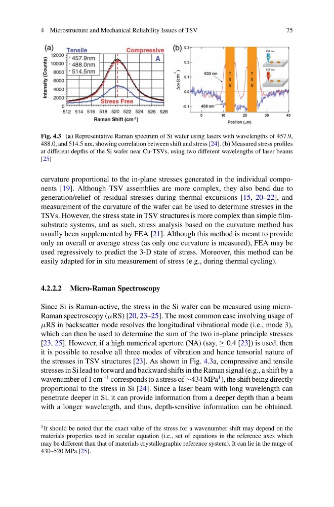
Fig. 4.3 (a) Representative Raman spectrum of Si wafer using lasers with wavelengths of 457.9,
488.0, and 514.5 nm, showing correlation between shift and stress [24]. (b) Measured stress profiles
at different depths of the Si wafer near Cu-TSVs, using two different wavelengths of laser beams
[25]
curvature proportional to the in-plane stresses generated in the individual components [19]. Although TSV assemblies are more complex, they also bend due to
generation/relief of residual stresses during thermal excursions [15, 20–22], and
measurement of the curvature of the wafer can be used to determine stresses in the
TSVs. However, the stress state in TSV structures is more complex than simple filmsubstrate systems, and as such, stress analysis based on the curvature method has
usually been supplemented by FEA [21]. Although this method is meant to provide
only an overall or average stress (as only one curvature is measured), FEA may be
used regressively to predict the 3-D state of stress. Moreover, this method can be
easily adapted for in situ measurement of stress (e.g., during thermal cycling).
4.2.2.2 Micro-Raman Spectroscopy
Since Si is Raman-active, the stress in the Si wafer can be measured using microRaman spectroscopy (μRS) [20, 23–25]. The most common case involving usage of
μRS in backscatter mode resolves the longitudinal vibrational mode (i.e., mode 3),
which can then be used to determine the sum of the two in-plane principle stresses
[23, 25]. However, if a high numerical aperture (NA) (say, ≥ 0.4 [23]) is used, then
it is possible to resolve all three modes of vibration and hence tensorial nature of
the stresses in TSV structures [23]. As shown in Fig. 4.3a, compressive and tensile
stresses in Si lead to forward and backward shifts in the Raman signal (e.g., a shift by a
wavenumber of 1 cm
−1 corresponds to a stress of ∼434 MPa
1 ), the shift being directly
proportional to the stress in Si [24]. Since a laser beam with long wavelength can
penetrate deeper in Si, it can provide information from a deeper depth than a beam
with a longer wavelength, and thus, depth-sensitive information can be obtained.
1 It should be noted that the exact value of the stress for a wavenumber shift may depend on the
materials properties used in secular equation (i.e., set of equations in the reference axes which
may be different than that of materials crystallographic reference system). It can lie in the range of
430–520 MPa [25].
75
Fig. 4.3 (a) Representative Raman spectrum of Si wafer using lasers with wavelengths of 457.9,
488.0, and 514.5 nm, showing correlation between shift and stress [24]. (b) Measured stress profiles
at different depths of the Si wafer near Cu-TSVs, using two different wavelengths of laser beams
[25]
curvature proportional to the in-plane stresses generated in the individual components [19]. Although TSV assemblies are more complex, they also bend due to
generation/relief of residual stresses during thermal excursions [15, 20–22], and
measurement of the curvature of the wafer can be used to determine stresses in the
TSVs. However, the stress state in TSV structures is more complex than simple filmsubstrate systems, and as such, stress analysis based on the curvature method has
usually been supplemented by FEA [21]. Although this method is meant to provide
only an overall or average stress (as only one curvature is measured), FEA may be
used regressively to predict the 3-D state of stress. Moreover, this method can be
easily adapted for in situ measurement of stress (e.g., during thermal cycling).
4.2.2.2 Micro-Raman Spectroscopy
Since Si is Raman-active, the stress in the Si wafer can be measured using microRaman spectroscopy (μRS) [20, 23–25]. The most common case involving usage of
μRS in backscatter mode resolves the longitudinal vibrational mode (i.e., mode 3),
which can then be used to determine the sum of the two in-plane principle stresses
[23, 25]. However, if a high numerical aperture (NA) (say, ≥ 0.4 [23]) is used, then
it is possible to resolve all three modes of vibration and hence tensorial nature of
the stresses in TSV structures [23]. As shown in Fig. 4.3a, compressive and tensile
stresses in Si lead to forward and backward shifts in the Raman signal (e.g., a shift by a
wavenumber of 1 cm
−1 corresponds to a stress of ∼434 MPa
1 ), the shift being directly
proportional to the stress in Si [24]. Since a laser beam with long wavelength can
penetrate deeper in Si, it can provide information from a deeper depth than a beam
with a longer wavelength, and thus, depth-sensitive information can be obtained.
1 It should be noted that the exact value of the stress for a wavenumber shift may depend on the
materials properties used in secular equation (i.e., set of equations in the reference axes which
may be different than that of materials crystallographic reference system). It can lie in the range of
430–520 MPa [25].