

50
P. Kumar et al.
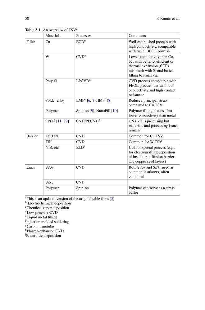
Table 3.1 An overview of TSV a
Materials
Processes
Comments
Filler
Cu
ECD b
Well-established process with
high conductivity, compatible
with metal BEOL process
W
CVD c
Lower conductivity than Cu,
but with better coefficient of
thermal expansion (CTE)
mismatch with Si and better
filling to small via
Poly-Si
LPCVD d
CVD process compatible with
FEOL process, but with low
conductivity and high contact
resistance
Solder alloy
LMF e [6, 7], IMS f [8]
Reduced principal stress
compared to Cu TSV
Polymer
Spin-on [9], NanoFill [10]
Polymer filling process, but
lower conductivity than metal
CNT g [11, 12]
CVD/PECVD h
CNT via is promising but
materials and processing issues
remain
Barrier
Ta, TaN
CVD
Common for Cu TSV
TiN
CVD
Common for W TSV
NiB, etc.
ELD i
Ued for special process (e.g.,
for electrografting deposition
of insulator, diffusion barrier
and copper seed layers)
Liner
SiO 2
CVD
Both SiO 2 and SiN x used as
common insulators, often
combined
SiN x
CVD
Polymer
Spin-on
Polymer can serve as a stress
buffer
a This is an updated version of the original table from [5]
b Electrochemical deposition
c Chemical vapor deposition
d Low-pressure CVD
e Liquid metal filling
f Injection molded soldering
g Carbon nanotube
h Plasma-enhanced CVD
i Electroless deposition
P. Kumar et al.
Table 3.1 An overview of TSV a
Materials
Processes
Comments
Filler
Cu
ECD b
Well-established process with
high conductivity, compatible
with metal BEOL process
W
CVD c
Lower conductivity than Cu,
but with better coefficient of
thermal expansion (CTE)
mismatch with Si and better
filling to small via
Poly-Si
LPCVD d
CVD process compatible with
FEOL process, but with low
conductivity and high contact
resistance
Solder alloy
LMF e [6, 7], IMS f [8]
Reduced principal stress
compared to Cu TSV
Polymer
Spin-on [9], NanoFill [10]
Polymer filling process, but
lower conductivity than metal
CNT g [11, 12]
CVD/PECVD h
CNT via is promising but
materials and processing issues
remain
Barrier
Ta, TaN
CVD
Common for Cu TSV
TiN
CVD
Common for W TSV
NiB, etc.
ELD i
Ued for special process (e.g.,
for electrografting deposition
of insulator, diffusion barrier
and copper seed layers)
Liner
SiO 2
CVD
Both SiO 2 and SiN x used as
common insulators, often
combined
SiN x
CVD
Polymer
Spin-on
Polymer can serve as a stress
buffer
a This is an updated version of the original table from [5]
b Electrochemical deposition
c Chemical vapor deposition
d Low-pressure CVD
e Liquid metal filling
f Injection molded soldering
g Carbon nanotube
h Plasma-enhanced CVD
i Electroless deposition