

606
Y. Li and D. Goyal
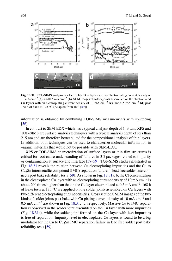
Fig. 18.31 TOF-SIMS analysis of electroplated Cu layers with an electroplating current density of
10 mA cm −2 (a), and 0.5 mA cm −2 (b). SEM images of solder joints assembled on the electroplated
Cu layers with an electroplating current density of 10 mA cm −2 (c), and 0.5 mA cm −2 (d) post
168 h of bake at 175 °C (Adapted from Ref. [59])
information is obtained by combining TOF-SIMS measurements with sputtering
[56].
In contrast to SEM-EDX which has a typical analysis depth of 1–3 μm, XPS and
TOF-SIMS are surface analysis techniques with a typical analysis depth of less than
2–5 nm and are therefore better suited for the compositional analysis of thin layers.
In addition, both techniques can be used to characterize molecular information in
organic materials that would not be possible with SEM-EDX.
XPS or TOF-SIMS characterization of surface layers or thin film structures is
critical for root-cause understanding of failures in 3D packages related to impurity
or contamination at surface and interface [57–59]. TOF-SIMS studies illustrated in
Fig. 18.31 reveals the relation between Cu electroplating impurities and the Cu to
Cu 3 Sn intermetallic compound (IMC) separation failure in lead free solder interconnects post bake reliability tests [59]. As shown in Fig. 18.31a, b, the Cl concentration
in the electroplated Cu layer with an electroplating current density of 10 mA cm
−2 is
about 200 times higher than that in the Cu layer electroplated at 0.5 mA cm
−2 . 168 h
of Bake tests at 175 °C are applied on the solder joints assembled on Cu layers with
two different electroplating current densities. Cross sectional SEM images of the two
kinds of solder joints post bake with Cu plating current density of 10 mA cm
−2 and
0.5 mA cm
−2 are shown in Fig. 18.31c, d, respectively. Massive Cu to IMC separation is observed in the solder joint assembled on the Cu layer with more impurities
(Fig. 18.31c), while the solder joint formed on the Cu layer with less impurities
is free of separation. Impurity level in electroplated Cu layers is found to be a big
modulator for the Cu to Cu 3 Sn IMC separation failure in lead free solder post bake
reliability tests [59].