

18 Fault Isolation and Failure Analysis of 3D Packaging
579
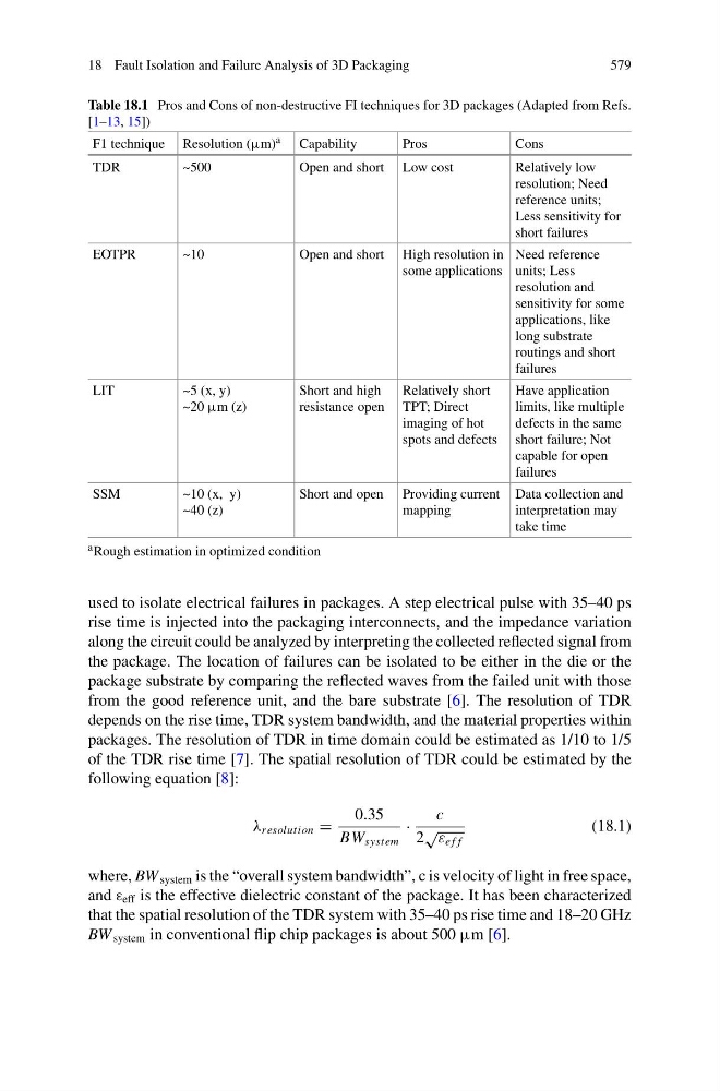
Table 18.1 Pros and Cons of non-destructive FI techniques for 3D packages (Adapted from Refs.
[1–13, 15])
F1 technique Resolution (μm) a Capability
Pros
Cons
TDR
~500
Open and short Low cost
Relatively low
resolution; Need
reference units;
Less sensitivity for
short failures
EOTPR
~10
Open and short High resolution in
some applications
Need reference
units; Less
resolution and
sensitivity for some
applications, like
long substrate
routings and short
failures
LIT
~5 (x, y)
~20 μm (z)
Short and high
resistance open
Relatively short
TPT; Direct
imaging of hot
spots and defects
Have application
limits, like multiple
defects in the same
short failure; Not
capable for open
failures
SSM
~10 (x, y)
~40 (z)
Short and open Providing current
mapping
Data collection and
interpretation may
take time
a Rough estimation in optimized condition
used to isolate electrical failures in packages. A step electrical pulse with 35–40 ps
rise time is injected into the packaging interconnects, and the impedance variation
along the circuit could be analyzed by interpreting the collected reflected signal from
the package. The location of failures can be isolated to be either in the die or the
package substrate by comparing the reflected waves from the failed unit with those
from the good reference unit, and the bare substrate [6]. The resolution of TDR
depends on the rise time, TDR system bandwidth, and the material properties within
packages. The resolution of TDR in time domain could be estimated as 1/10 to 1/5
of the TDR rise time [7]. The spatial resolution of TDR could be estimated by the
following equation [8]:
λ resolution =
0.35
BW system
·
c
2
√ ε e f f
(18.1)
where, BW system is the “overall system bandwidth”, c is velocity of light in free space,
and ε eff is the effective dielectric constant of the package. It has been characterized
that the spatial resolution of the TDR system with 35–40 ps rise time and 18–20 GHz
BW system in conventional flip chip packages is about 500 μm [6].
579
Table 18.1 Pros and Cons of non-destructive FI techniques for 3D packages (Adapted from Refs.
[1–13, 15])
F1 technique Resolution (μm) a Capability
Pros
Cons
TDR
~500
Open and short Low cost
Relatively low
resolution; Need
reference units;
Less sensitivity for
short failures
EOTPR
~10
Open and short High resolution in
some applications
Need reference
units; Less
resolution and
sensitivity for some
applications, like
long substrate
routings and short
failures
LIT
~5 (x, y)
~20 μm (z)
Short and high
resistance open
Relatively short
TPT; Direct
imaging of hot
spots and defects
Have application
limits, like multiple
defects in the same
short failure; Not
capable for open
failures
SSM
~10 (x, y)
~40 (z)
Short and open Providing current
mapping
Data collection and
interpretation may
take time
a Rough estimation in optimized condition
used to isolate electrical failures in packages. A step electrical pulse with 35–40 ps
rise time is injected into the packaging interconnects, and the impedance variation
along the circuit could be analyzed by interpreting the collected reflected signal from
the package. The location of failures can be isolated to be either in the die or the
package substrate by comparing the reflected waves from the failed unit with those
from the good reference unit, and the bare substrate [6]. The resolution of TDR
depends on the rise time, TDR system bandwidth, and the material properties within
packages. The resolution of TDR in time domain could be estimated as 1/10 to 1/5
of the TDR rise time [7]. The spatial resolution of TDR could be estimated by the
following equation [8]:
λ resolution =
0.35
BW system
·
c
2
√ ε e f f
(18.1)
where, BW system is the “overall system bandwidth”, c is velocity of light in free space,
and ε eff is the effective dielectric constant of the package. It has been characterized
that the spatial resolution of the TDR system with 35–40 ps rise time and 18–20 GHz
BW system in conventional flip chip packages is about 500 μm [6].