

534
Y. Wang et al.
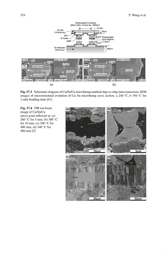
Fig. 17.3 Schematic diagram of Cu/Sn/Cu microbump enabled chip-to-chip interconnection; SEM
images of microstructural evolution of Cu–Sn microbump cross section. a 240 °C, b 350 °C for
1-min bonding time [81]
Fig. 17.4 FIB ion beam
image of Cu/Sn/Cu
micro-joint reflowed at: (a)
260 °C for 5 min; (b) 300 °C
for 10 min; (c) 300 °C for
480 min; (d) 340 °C for
480 min [5]
Y. Wang et al.
Fig. 17.3 Schematic diagram of Cu/Sn/Cu microbump enabled chip-to-chip interconnection; SEM
images of microstructural evolution of Cu–Sn microbump cross section. a 240 °C, b 350 °C for
1-min bonding time [81]
Fig. 17.4 FIB ion beam
image of Cu/Sn/Cu
micro-joint reflowed at: (a)
260 °C for 5 min; (b) 300 °C
for 10 min; (c) 300 °C for
480 min; (d) 340 °C for
480 min [5]