

532
Y. Wang et al.
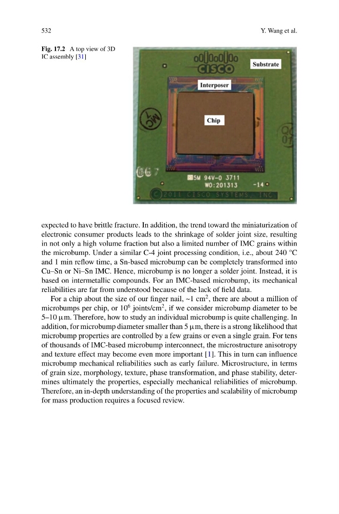
Fig. 17.2 A top view of 3D
IC assembly [31]
expected to have brittle fracture. In addition, the trend toward the miniaturization of
electronic consumer products leads to the shrinkage of solder joint size, resulting
in not only a high volume fraction but also a limited number of IMC grains within
the microbump. Under a similar C-4 joint processing condition, i.e., about 240 °C
and 1 min reflow time, a Sn-based microbump can be completely transformed into
Cu–Sn or Ni–Sn IMC. Hence, microbump is no longer a solder joint. Instead, it is
based on intermetallic compounds. For an IMC-based microbump, its mechanical
reliabilities are far from understood because of the lack of field data.
For a chip about the size of our finger nail, ~1 cm
2 , there are about a million of
microbumps per chip, or 10
6 joints/cm
2 , if we consider microbump diameter to be
5–10 μm. Therefore, how to study an individual microbump is quite challenging. In
addition, for microbump diameter smaller than 5 μm, there is a strong likelihood that
microbump properties are controlled by a few grains or even a single grain. For tens
of thousands of IMC-based microbump interconnect, the microstructure anisotropy
and texture effect may become even more important [1]. This in turn can influence
microbump mechanical reliabilities such as early failure. Microstructure, in terms
of grain size, morphology, texture, phase transformation, and phase stability, determines ultimately the properties, especially mechanical reliabilities of microbump.
Therefore, an in-depth understanding of the properties and scalability of microbump
for mass production requires a focused review.
Y. Wang et al.
Fig. 17.2 A top view of 3D
IC assembly [31]
expected to have brittle fracture. In addition, the trend toward the miniaturization of
electronic consumer products leads to the shrinkage of solder joint size, resulting
in not only a high volume fraction but also a limited number of IMC grains within
the microbump. Under a similar C-4 joint processing condition, i.e., about 240 °C
and 1 min reflow time, a Sn-based microbump can be completely transformed into
Cu–Sn or Ni–Sn IMC. Hence, microbump is no longer a solder joint. Instead, it is
based on intermetallic compounds. For an IMC-based microbump, its mechanical
reliabilities are far from understood because of the lack of field data.
For a chip about the size of our finger nail, ~1 cm
2 , there are about a million of
microbumps per chip, or 10
6 joints/cm
2 , if we consider microbump diameter to be
5–10 μm. Therefore, how to study an individual microbump is quite challenging. In
addition, for microbump diameter smaller than 5 μm, there is a strong likelihood that
microbump properties are controlled by a few grains or even a single grain. For tens
of thousands of IMC-based microbump interconnect, the microstructure anisotropy
and texture effect may become even more important [1]. This in turn can influence
microbump mechanical reliabilities such as early failure. Microstructure, in terms
of grain size, morphology, texture, phase transformation, and phase stability, determines ultimately the properties, especially mechanical reliabilities of microbump.
Therefore, an in-depth understanding of the properties and scalability of microbump
for mass production requires a focused review.