

36
R. Mahajan and B. Sankman
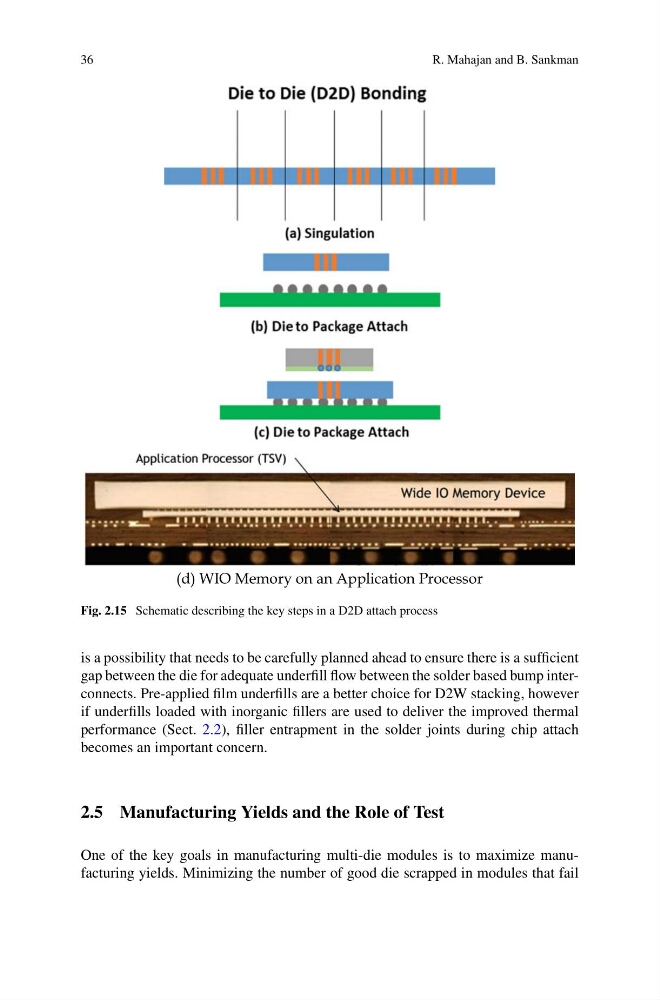
(d) WIO Memory on an Application Processor
Fig. 2.15 Schematic describing the key steps in a D2D attach process
is a possibility that needs to be carefully planned ahead to ensure there is a sufficient
gap between the die for adequate underfill flow between the solder based bump interconnects. Pre-applied film underfills are a better choice for D2W stacking, however
if underfills loaded with inorganic fillers are used to deliver the improved thermal
performance (Sect. 2.2), filler entrapment in the solder joints during chip attach
becomes an important concern.
2.5 Manufacturing Yields and the Role of Test
One of the key goals in manufacturing multi-die modules is to maximize manufacturing yields. Minimizing the number of good die scrapped in modules that fail
R. Mahajan and B. Sankman
(d) WIO Memory on an Application Processor
Fig. 2.15 Schematic describing the key steps in a D2D attach process
is a possibility that needs to be carefully planned ahead to ensure there is a sufficient
gap between the die for adequate underfill flow between the solder based bump interconnects. Pre-applied film underfills are a better choice for D2W stacking, however
if underfills loaded with inorganic fillers are used to deliver the improved thermal
performance (Sect. 2.2), filler entrapment in the solder joints during chip attach
becomes an important concern.
2.5 Manufacturing Yields and the Role of Test
One of the key goals in manufacturing multi-die modules is to maximize manufacturing yields. Minimizing the number of good die scrapped in modules that fail