

528
Y. Wang et al.
of voids in a brittle material can easily lead to fracture damage [2]. The interest in
mechanical failures is because for mobile and wearable devices, the frequency of
impact and dropping to the ground is high. On EM and TM in microbumps, we
emphasize the enhanced failure mode due to Joule heating.
17.2 Quality Challenges for 3D Packaging
3D IC devices involves more complicated stacking processes where interconnect size
becomes much smaller. Materials properties used in 3D-IC influence the quality and
reliability of electronic assemblies. For example, PCB substrate, silicon, microbump,
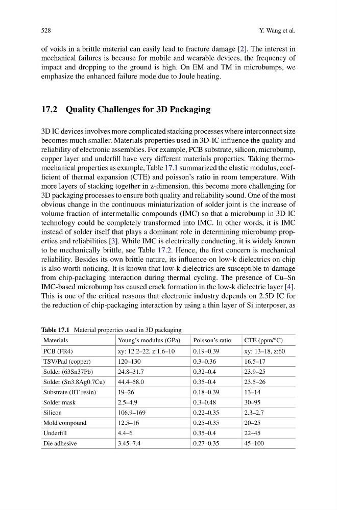
copper layer and underfill have very different materials properties. Taking thermomechanical properties as example, Table 17.1 summarized the elastic modulus, coefficient of thermal expansion (CTE) and poisson’s ratio in room temperature. With
more layers of stacking together in z-dimension, this become more challenging for
3D packaging processes to ensure both quality and reliability sound. One of the most
obvious change in the continuous miniaturization of solder joint is the increase of
volume fraction of intermetallic compounds (IMC) so that a microbump in 3D IC
technology could be completely transformed into IMC. In other words, it is IMC
instead of solder itself that plays a dominant role in determining microbump properties and reliabilities [3]. While IMC is electrically conducting, it is widely known
to be mechanically brittle, see Table 17.2. Hence, the first concern is mechanical
reliability. Besides its own brittle nature, its influence on low-k dielectrics on chip
is also worth noticing. It is known that low-k dielectrics are susceptible to damage
from chip-packaging interaction during thermal cycling. The presence of Cu–Sn
IMC-based microbump has caused crack formation in the low-k dielectric layer [4].
This is one of the critical reasons that electronic industry depends on 2.5D IC for
the reduction of chip-packaging interaction by using a thin layer of Si interposer, as
Table 17.1 Material properties used in 3D packaging
Materials
Young’s modulus (GPa)
Poisson’s ratio
CTE (ppm/°C)
PCB (FR4)
xy: 12.2–22, z:1.6–10
0.19–0.39
xy: 13–18, z:60
TSV/Pad (copper)
120–130
0.3–0.36
16.5–17
Solder (63Sn37Pb)
24.8–31.7
0.32–0.4
23.9–25
Solder (Sn3.8Ag0.7Cu)
44.4–58.0
0.35–0.4
23.5–26
Substrate (BT resin)
19–26
0.18–0.39
13–14
Solder mask
2.5–4.9
0.3–0.48
30–95
Silicon
106.9–169
0.22–0.35
2.3–2.7
Mold compound
12.5–16
0.25–0.35
20–25
Underfill
4.4–6
0.35–0.4
22–45
Die adhesive
3.45–7.4
0.27–0.35
45–100
Y. Wang et al.
of voids in a brittle material can easily lead to fracture damage [2]. The interest in
mechanical failures is because for mobile and wearable devices, the frequency of
impact and dropping to the ground is high. On EM and TM in microbumps, we
emphasize the enhanced failure mode due to Joule heating.
17.2 Quality Challenges for 3D Packaging
3D IC devices involves more complicated stacking processes where interconnect size
becomes much smaller. Materials properties used in 3D-IC influence the quality and
reliability of electronic assemblies. For example, PCB substrate, silicon, microbump,
copper layer and underfill have very different materials properties. Taking thermomechanical properties as example, Table 17.1 summarized the elastic modulus, coefficient of thermal expansion (CTE) and poisson’s ratio in room temperature. With
more layers of stacking together in z-dimension, this become more challenging for
3D packaging processes to ensure both quality and reliability sound. One of the most
obvious change in the continuous miniaturization of solder joint is the increase of
volume fraction of intermetallic compounds (IMC) so that a microbump in 3D IC
technology could be completely transformed into IMC. In other words, it is IMC
instead of solder itself that plays a dominant role in determining microbump properties and reliabilities [3]. While IMC is electrically conducting, it is widely known
to be mechanically brittle, see Table 17.2. Hence, the first concern is mechanical
reliability. Besides its own brittle nature, its influence on low-k dielectrics on chip
is also worth noticing. It is known that low-k dielectrics are susceptible to damage
from chip-packaging interaction during thermal cycling. The presence of Cu–Sn
IMC-based microbump has caused crack formation in the low-k dielectric layer [4].
This is one of the critical reasons that electronic industry depends on 2.5D IC for
the reduction of chip-packaging interaction by using a thin layer of Si interposer, as
Table 17.1 Material properties used in 3D packaging
Materials
Young’s modulus (GPa)
Poisson’s ratio
CTE (ppm/°C)
PCB (FR4)
xy: 12.2–22, z:1.6–10
0.19–0.39
xy: 13–18, z:60
TSV/Pad (copper)
120–130
0.3–0.36
16.5–17
Solder (63Sn37Pb)
24.8–31.7
0.32–0.4
23.9–25
Solder (Sn3.8Ag0.7Cu)
44.4–58.0
0.35–0.4
23.5–26
Substrate (BT resin)
19–26
0.18–0.39
13–14
Solder mask
2.5–4.9
0.3–0.48
30–95
Silicon
106.9–169
0.22–0.35
2.3–2.7
Mold compound
12.5–16
0.25–0.35
20–25
Underfill
4.4–6
0.35–0.4
22–45
Die adhesive
3.45–7.4
0.27–0.35
45–100