

486
P. Vianco and M. Neilsen
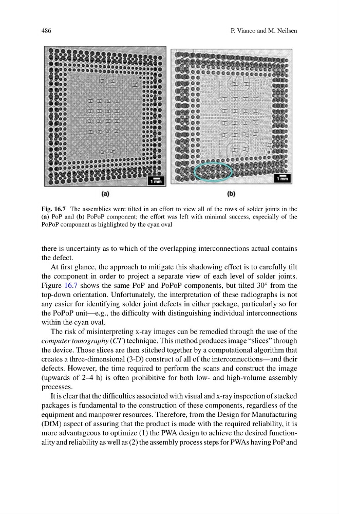
Fig. 16.7 The assemblies were tilted in an effort to view all of the rows of solder joints in the
(a) PoP and (b) PoPoP component; the effort was left with minimal success, especially of the
PoPoP component as highlighted by the cyan oval
there is uncertainty as to which of the overlapping interconnections actual contains
the defect.
At first glance, the approach to mitigate this shadowing effect is to carefully tilt
the component in order to project a separate view of each level of solder joints.
Figure 16.7 shows the same PoP and PoPoP components, but tilted 30° from the
top-down orientation. Unfortunately, the interpretation of these radiographs is not
any easier for identifying solder joint defects in either package, particularly so for
the PoPoP unit—e.g., the difficulty with distinguishing individual interconnections
within the cyan oval.
The risk of misinterpreting x-ray images can be remedied through the use of the
computer tomography (CT ) technique. This method produces image “slices” through
the device. Those slices are then stitched together by a computational algorithm that
creates a three-dimensional (3-D) construct of all of the interconnections—and their
defects. However, the time required to perform the scans and construct the image
(upwards of 2–4 h) is often prohibitive for both low- and high-volume assembly
processes.
It is clear that the difficulties associated with visual and x-ray inspection of stacked
packages is fundamental to the construction of these components, regardless of the
equipment and manpower resources. Therefore, from the Design for Manufacturing
(DfM) aspect of assuring that the product is made with the required reliability, it is
more advantageous to optimize (1) the PWA design to achieve the desired functionality and reliability as well as (2) the assembly process steps for PWAs having PoP and
P. Vianco and M. Neilsen
Fig. 16.7 The assemblies were tilted in an effort to view all of the rows of solder joints in the
(a) PoP and (b) PoPoP component; the effort was left with minimal success, especially of the
PoPoP component as highlighted by the cyan oval
there is uncertainty as to which of the overlapping interconnections actual contains
the defect.
At first glance, the approach to mitigate this shadowing effect is to carefully tilt
the component in order to project a separate view of each level of solder joints.
Figure 16.7 shows the same PoP and PoPoP components, but tilted 30° from the
top-down orientation. Unfortunately, the interpretation of these radiographs is not
any easier for identifying solder joint defects in either package, particularly so for
the PoPoP unit—e.g., the difficulty with distinguishing individual interconnections
within the cyan oval.
The risk of misinterpreting x-ray images can be remedied through the use of the
computer tomography (CT ) technique. This method produces image “slices” through
the device. Those slices are then stitched together by a computational algorithm that
creates a three-dimensional (3-D) construct of all of the interconnections—and their
defects. However, the time required to perform the scans and construct the image
(upwards of 2–4 h) is often prohibitive for both low- and high-volume assembly
processes.
It is clear that the difficulties associated with visual and x-ray inspection of stacked
packages is fundamental to the construction of these components, regardless of the
equipment and manpower resources. Therefore, from the Design for Manufacturing
(DfM) aspect of assuring that the product is made with the required reliability, it is
more advantageous to optimize (1) the PWA design to achieve the desired functionality and reliability as well as (2) the assembly process steps for PWAs having PoP and