

474
P. Vianco and M. Neilsen
that stacks two (2) packages atop each other, and package-on-package-on-package
(PoPoP) that is a three-package stack. Any needs for further miniaturization cause
the stacked packaging option to give way to the stacked die technology.
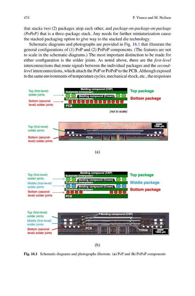
Schematic diagrams and photographs are provided in Fig. 16.1 that illustrate the
general configurations of (1) PoP and (2) PoPoP components. (The features are not
to scale in the schematic diagrams.) The most important distinction to be made for
either configuration is the solder joints. As noted above, there are the first-level
interconnections that route signals between the individual packages and the secondlevel interconnections, which attach the PoP or PoPoP to the PCB. Although exposed
to the same environments of temperature cycles, mechanical shock, etc., the responses
Fig. 16.1 Schematic diagrams and photographs illustrate. (a) PoP and (b) PoPoP components
P. Vianco and M. Neilsen
that stacks two (2) packages atop each other, and package-on-package-on-package
(PoPoP) that is a three-package stack. Any needs for further miniaturization cause
the stacked packaging option to give way to the stacked die technology.
Schematic diagrams and photographs are provided in Fig. 16.1 that illustrate the
general configurations of (1) PoP and (2) PoPoP components. (The features are not
to scale in the schematic diagrams.) The most important distinction to be made for
either configuration is the solder joints. As noted above, there are the first-level
interconnections that route signals between the individual packages and the secondlevel interconnections, which attach the PoP or PoPoP to the PCB. Although exposed
to the same environments of temperature cycles, mechanical shock, etc., the responses
Fig. 16.1 Schematic diagrams and photographs illustrate. (a) PoP and (b) PoPoP components