

15 Die and Package Level Thermal and Thermal/Moisture Stresses …
443
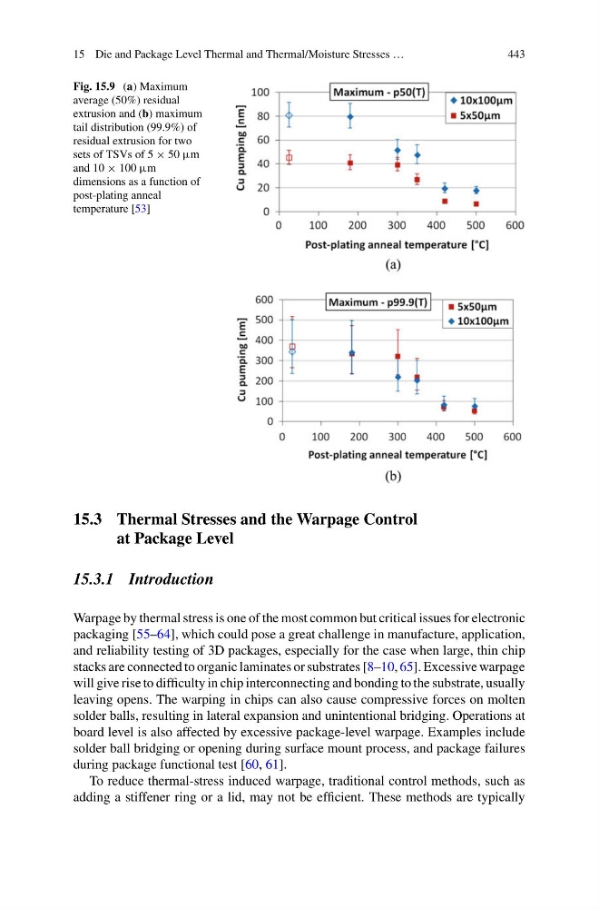
Fig. 15.9 (a) Maximum
average (50%) residual
extrusion and (b) maximum
tail distribution (99.9%) of
residual extrusion for two
sets of TSVs of 5 × 50 μm
and 10 × 100 μm
dimensions as a function of
post-plating anneal
temperature [53]
15.3 Thermal Stresses and the Warpage Control
at Package Level
15.3.1 Introduction
Warpage by thermal stress is one of the most common but critical issues for electronic
packaging [55–64], which could pose a great challenge in manufacture, application,
and reliability testing of 3D packages, especially for the case when large, thin chip
stacks are connected to organic laminates or substrates [8–10, 65]. Excessive warpage
will give rise to difficulty in chip interconnecting and bonding to the substrate, usually
leaving opens. The warping in chips can also cause compressive forces on molten
solder balls, resulting in lateral expansion and unintentional bridging. Operations at
board level is also affected by excessive package-level warpage. Examples include
solder ball bridging or opening during surface mount process, and package failures
during package functional test [60, 61].
To reduce thermal-stress induced warpage, traditional control methods, such as
adding a stiffener ring or a lid, may not be efficient. These methods are typically
443
Fig. 15.9 (a) Maximum
average (50%) residual
extrusion and (b) maximum
tail distribution (99.9%) of
residual extrusion for two
sets of TSVs of 5 × 50 μm
and 10 × 100 μm
dimensions as a function of
post-plating anneal
temperature [53]
15.3 Thermal Stresses and the Warpage Control
at Package Level
15.3.1 Introduction
Warpage by thermal stress is one of the most common but critical issues for electronic
packaging [55–64], which could pose a great challenge in manufacture, application,
and reliability testing of 3D packages, especially for the case when large, thin chip
stacks are connected to organic laminates or substrates [8–10, 65]. Excessive warpage
will give rise to difficulty in chip interconnecting and bonding to the substrate, usually
leaving opens. The warping in chips can also cause compressive forces on molten
solder balls, resulting in lateral expansion and unintentional bridging. Operations at
board level is also affected by excessive package-level warpage. Examples include
solder ball bridging or opening during surface mount process, and package failures
during package functional test [60, 61].
To reduce thermal-stress induced warpage, traditional control methods, such as
adding a stiffener ring or a lid, may not be efficient. These methods are typically