

14 Fundamentals of Advanced Materials …
423
Incoming core with
Copper clad
UV
UV
Through hole drill
FLI formation (uball or paste printed solder).
Repeat semi-additive process as per the product stack up,
till SR lamination, Exposure, Develop, Cure, Plasma clean,
surface finish plating.
Copper roughening, Di-electric Lamination, Cure, Laser drilling, Semi additive process
( Via cleaning, Seed layer plating, DFR lamination, exposure, develop,
Cu plating, DFR stripping, Seed Layer etch).
Second Layer Patterning following the
same steps as first layer (Subtractive).
Through hole plugging, Cure, Grinding,
Lid plating
Copper Roughening, Insulation layer lamination, Cure, Mechanical
drilling, through hole cleaning, seed layer plating, E-lytic Cu plating.
First Layer patterning, Subtractive etching ( Photoresist lamination, Exposure, develop, Etching, DFR Stripping)
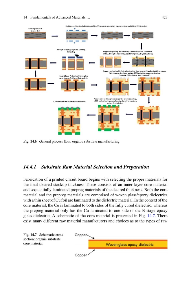
Fig. 14.6 General process flow: organic substrate manufacturing
14.4.1 Substrate Raw Material Selection and Preparation
Fabrication of a printed circuit board begins with selecting the proper materials for
the final desired stackup thickness These consists of an inner layer core material
and sequentially laminated prepreg materials of the desired thickness. Both the core
material and the prepreg materials are comprised of woven glass/epoxy dielectrics
with a thin sheet of Cu foil are laminated to the dielectric material. In the context of the
core material, the Cu is laminated to both sides of the fully cured dielectric, whereas
the prepreg material only has the Cu laminated to one side of the B-stage epoxy
glass dielectric. A schematic of the core material is presented in Fig. 14.7. There
exist many different raw material manufacturers and choices as to the types of raw
Fig. 14.7 Schematic cross
section: organic substrate
core material
423
Incoming core with
Copper clad
UV
UV
Through hole drill
FLI formation (uball or paste printed solder).
Repeat semi-additive process as per the product stack up,
till SR lamination, Exposure, Develop, Cure, Plasma clean,
surface finish plating.
Copper roughening, Di-electric Lamination, Cure, Laser drilling, Semi additive process
( Via cleaning, Seed layer plating, DFR lamination, exposure, develop,
Cu plating, DFR stripping, Seed Layer etch).
Second Layer Patterning following the
same steps as first layer (Subtractive).
Through hole plugging, Cure, Grinding,
Lid plating
Copper Roughening, Insulation layer lamination, Cure, Mechanical
drilling, through hole cleaning, seed layer plating, E-lytic Cu plating.
First Layer patterning, Subtractive etching ( Photoresist lamination, Exposure, develop, Etching, DFR Stripping)
Fig. 14.6 General process flow: organic substrate manufacturing
14.4.1 Substrate Raw Material Selection and Preparation
Fabrication of a printed circuit board begins with selecting the proper materials for
the final desired stackup thickness These consists of an inner layer core material
and sequentially laminated prepreg materials of the desired thickness. Both the core
material and the prepreg materials are comprised of woven glass/epoxy dielectrics
with a thin sheet of Cu foil are laminated to the dielectric material. In the context of the
core material, the Cu is laminated to both sides of the fully cured dielectric, whereas
the prepreg material only has the Cu laminated to one side of the B-stage epoxy
glass dielectric. A schematic of the core material is presented in Fig. 14.7. There
exist many different raw material manufacturers and choices as to the types of raw
Fig. 14.7 Schematic cross
section: organic substrate
core material