

12 Fundamentals of Electromigration in Interconnects of 3D Packaging
363
cathode and anode. Besides that, the complexity of design structures, manufacture processes and dielectric materials for Cu interconnects can also induce
thermal mechanical stress gradient due to thermal mismatch at high temperature EM testing. It has been reported that passivation layer thickness [52] and
interconnect processing temperature [53] can dramatically modulate the thermal
stress gradients in metal lines and change their EM performance.
12.4.2 EM Failure in TSV
In a recent study, Oba et al. [54] reported the EM testing on a typical TSV structure.
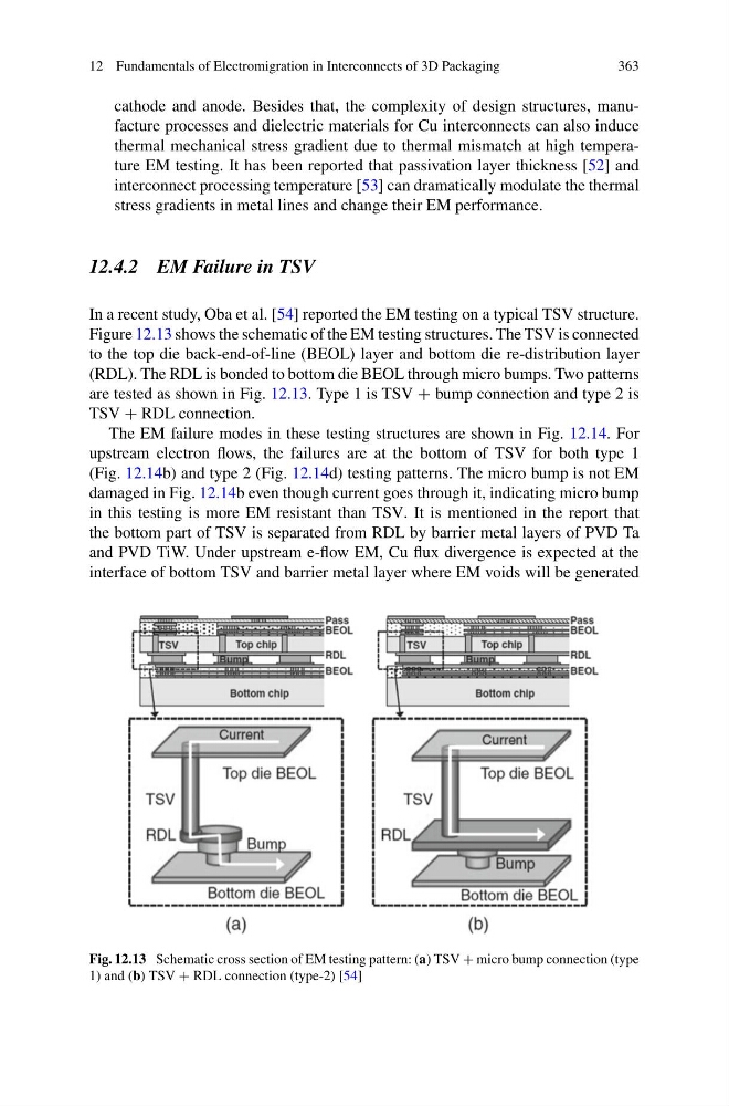
Figure 12.13 shows the schematic of the EM testing structures. The TSV is connected
to the top die back-end-of-line (BEOL) layer and bottom die re-distribution layer
(RDL). The RDL is bonded to bottom die BEOL through micro bumps. Two patterns
are tested as shown in Fig. 12.13. Type 1 is TSV + bump connection and type 2 is
TSV + RDL connection.
The EM failure modes in these testing structures are shown in Fig. 12.14. For
upstream electron flows, the failures are at the bottom of TSV for both type 1
(Fig. 12.14b) and type 2 (Fig. 12.14d) testing patterns. The micro bump is not EM
damaged in Fig. 12.14b even though current goes through it, indicating micro bump
in this testing is more EM resistant than TSV. It is mentioned in the report that
the bottom part of TSV is separated from RDL by barrier metal layers of PVD Ta
and PVD TiW. Under upstream e-flow EM, Cu flux divergence is expected at the
interface of bottom TSV and barrier metal layer where EM voids will be generated
Fig. 12.13 Schematic cross section of EM testing pattern: (a) TSV + micro bump connection (type
1) and (b) TSV + RDL connection (type-2) [54]
363
cathode and anode. Besides that, the complexity of design structures, manufacture processes and dielectric materials for Cu interconnects can also induce
thermal mechanical stress gradient due to thermal mismatch at high temperature EM testing. It has been reported that passivation layer thickness [52] and
interconnect processing temperature [53] can dramatically modulate the thermal
stress gradients in metal lines and change their EM performance.
12.4.2 EM Failure in TSV
In a recent study, Oba et al. [54] reported the EM testing on a typical TSV structure.
Figure 12.13 shows the schematic of the EM testing structures. The TSV is connected
to the top die back-end-of-line (BEOL) layer and bottom die re-distribution layer
(RDL). The RDL is bonded to bottom die BEOL through micro bumps. Two patterns
are tested as shown in Fig. 12.13. Type 1 is TSV + bump connection and type 2 is
TSV + RDL connection.
The EM failure modes in these testing structures are shown in Fig. 12.14. For
upstream electron flows, the failures are at the bottom of TSV for both type 1
(Fig. 12.14b) and type 2 (Fig. 12.14d) testing patterns. The micro bump is not EM
damaged in Fig. 12.14b even though current goes through it, indicating micro bump
in this testing is more EM resistant than TSV. It is mentioned in the report that
the bottom part of TSV is separated from RDL by barrier metal layers of PVD Ta
and PVD TiW. Under upstream e-flow EM, Cu flux divergence is expected at the
interface of bottom TSV and barrier metal layer where EM voids will be generated
Fig. 12.13 Schematic cross section of EM testing pattern: (a) TSV + micro bump connection (type
1) and (b) TSV + RDL connection (type-2) [54]