

348
P. Liu
will be discussed in Sect. 12.4 with the brief summaries about the key EM factors of
Cu damascene interconnects.
12.2 Key Modulators for EM in Solder Joints
EM can cause solder joint failures at IMC/solder interface due to flux divergence
induced by Sn self-diffusion, which is a very common EM failure mode and has
been well discussed [6–8]. On the other hand, electron wind can also accelerate the
dissolution of under bump metallization (UBM) on cathode side and cause failures
due to depletion of UBM [9, 10]. It has been reported that metallization dissolution
is closely related to Sn grain orientations [9, 10].
12.2.1 Typical EM Fail Caused by Sn Diffusion
In general, EM can induce failures through a void nucleation and propagation
mechanism. Voids nucleate near the entrance of electrons due to moving away of
the predominant diffusion species, which is caused by the momentum exchange
between electron wind and metal ions. The fundamental force equation governing
electro-migration is given by Eq. (12.1) [11].
F E M = Z
∗ eE = (Z
∗
el + Z
∗
wd )eρ j
(12.1)
where F EM stands for electro-migration driving force, Z* is effective charge representing transfer of momentum from electrons to atoms, e is electron charge, ρ is
resistively, j is current density, Z
*
el nominal valence of the diffusing ion for the direct
force and Z
*
wd is the effective valence for the electron wind force.
In Sn based Pb-free solders, the predominant diffusion specie is Sn atom and
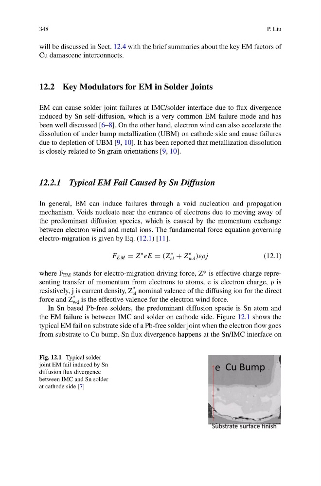
the EM failure is between IMC and solder on cathode side. Figure 12.1 shows the
typical EM fail on substrate side of a Pb-free solder joint when the electron flow goes
from substrate to Cu bump. Sn flux divergence happens at the Sn/IMC interface on
Fig. 12.1 Typical solder
joint EM fail induced by Sn
diffusion flux divergence
between IMC and Sn solder
at cathode side [7]
P. Liu
will be discussed in Sect. 12.4 with the brief summaries about the key EM factors of
Cu damascene interconnects.
12.2 Key Modulators for EM in Solder Joints
EM can cause solder joint failures at IMC/solder interface due to flux divergence
induced by Sn self-diffusion, which is a very common EM failure mode and has
been well discussed [6–8]. On the other hand, electron wind can also accelerate the
dissolution of under bump metallization (UBM) on cathode side and cause failures
due to depletion of UBM [9, 10]. It has been reported that metallization dissolution
is closely related to Sn grain orientations [9, 10].
12.2.1 Typical EM Fail Caused by Sn Diffusion
In general, EM can induce failures through a void nucleation and propagation
mechanism. Voids nucleate near the entrance of electrons due to moving away of
the predominant diffusion species, which is caused by the momentum exchange
between electron wind and metal ions. The fundamental force equation governing
electro-migration is given by Eq. (12.1) [11].
F E M = Z
∗ eE = (Z
∗
el + Z
∗
wd )eρ j
(12.1)
where F EM stands for electro-migration driving force, Z* is effective charge representing transfer of momentum from electrons to atoms, e is electron charge, ρ is
resistively, j is current density, Z
*
el nominal valence of the diffusing ion for the direct
force and Z
*
wd is the effective valence for the electron wind force.
In Sn based Pb-free solders, the predominant diffusion specie is Sn atom and
the EM failure is between IMC and solder on cathode side. Figure 12.1 shows the
typical EM fail on substrate side of a Pb-free solder joint when the electron flow goes
from substrate to Cu bump. Sn flux divergence happens at the Sn/IMC interface on
Fig. 12.1 Typical solder
joint EM fail induced by Sn
diffusion flux divergence
between IMC and Sn solder
at cathode side [7]