

11 Fundamentals of Solder Alloys in 3D Packaging
343
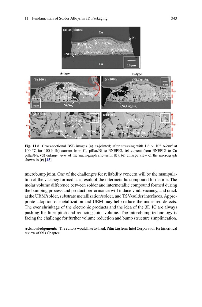
Fig. 11.8 Cross-sectional BSE images (a) as-jointed; after stressing with 1.8 × 10 4 A/cm 2 at
100 °C for 100 h (b) current from Cu pillar/Ni to ENEPIG, (c) current from ENEPIG to Cu
pillar/Ni, (d) enlarge view of the micrograph shown in (b), (e) enlarge view of the micrograph
shown in (c) [45]
microbump joint. One of the challenges for reliability concern will be the manipulation of the vacancy formed as a result of the intermetallic compound formation. The
molar volume difference between solder and intermetallic compound formed during
the bumping process and product performance will induce void, vacancy, and crack
at the UBM/solder, substrate metallization/solder, and TSV/solder interfaces. Appropriate adoption of metallization and UBM may help reduce the undesired defects.
The ever shrinkage of the electronic products and the idea of the 3D IC are always
pushing for finer pitch and reducing joint volume. The microbump technology is
facing the challenge for further volume reduction and bump structure simplification.
Acknowledgements The editors would like to thank Pilin Liu from Intel Corporation for his critical
review of this Chapter.
343
Fig. 11.8 Cross-sectional BSE images (a) as-jointed; after stressing with 1.8 × 10 4 A/cm 2 at
100 °C for 100 h (b) current from Cu pillar/Ni to ENEPIG, (c) current from ENEPIG to Cu
pillar/Ni, (d) enlarge view of the micrograph shown in (b), (e) enlarge view of the micrograph
shown in (c) [45]
microbump joint. One of the challenges for reliability concern will be the manipulation of the vacancy formed as a result of the intermetallic compound formation. The
molar volume difference between solder and intermetallic compound formed during
the bumping process and product performance will induce void, vacancy, and crack
at the UBM/solder, substrate metallization/solder, and TSV/solder interfaces. Appropriate adoption of metallization and UBM may help reduce the undesired defects.
The ever shrinkage of the electronic products and the idea of the 3D IC are always
pushing for finer pitch and reducing joint volume. The microbump technology is
facing the challenge for further volume reduction and bump structure simplification.
Acknowledgements The editors would like to thank Pilin Liu from Intel Corporation for his critical
review of this Chapter.