

11 Fundamentals of Solder Alloys in 3D Packaging
341
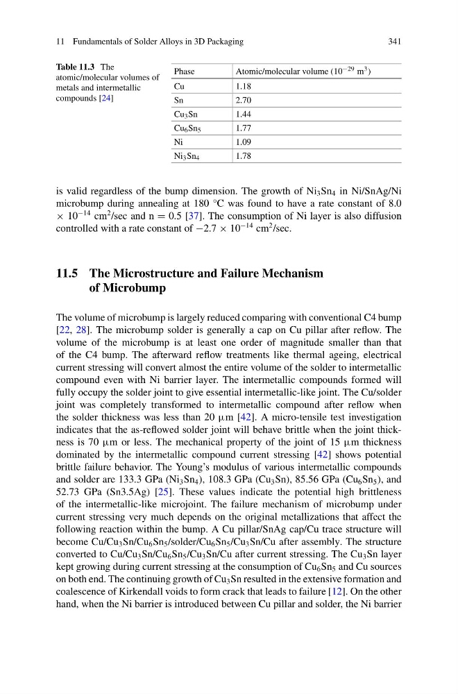
Table 11.3 The
atomic/molecular volumes of
metals and intermetallic
compounds [24]
Phase
Atomic/molecular volume (10 −29 m 3 )
Cu
1.18
Sn
2.70
Cu 3 Sn
1.44
Cu 6 Sn 5
1.77
Ni
1.09
Ni 3 Sn 4
1.78
is valid regardless of the bump dimension. The growth of Ni 3 Sn 4 in Ni/SnAg/Ni
microbump during annealing at 180 °C was found to have a rate constant of 8.0
× 10
−14 cm
2 /sec and n = 0.5 [37]. The consumption of Ni layer is also diffusion
controlled with a rate constant of −2.7 × 10
−14 cm
2 /sec.
11.5 The Microstructure and Failure Mechanism
of Microbump
The volume of microbump is largely reduced comparing with conventional C4 bump
[22, 28]. The microbump solder is generally a cap on Cu pillar after reflow. The
volume of the microbump is at least one order of magnitude smaller than that
of the C4 bump. The afterward reflow treatments like thermal ageing, electrical
current stressing will convert almost the entire volume of the solder to intermetallic
compound even with Ni barrier layer. The intermetallic compounds formed will
fully occupy the solder joint to give essential intermetallic-like joint. The Cu/solder
joint was completely transformed to intermetallic compound after reflow when
the solder thickness was less than 20 µm [42]. A micro-tensile test investigation
indicates that the as-reflowed solder joint will behave brittle when the joint thickness is 70 µm or less. The mechanical property of the joint of 15 µm thickness
dominated by the intermetallic compound current stressing [42] shows potential
brittle failure behavior. The Young’s modulus of various intermetallic compounds
and solder are 133.3 GPa (Ni 3 Sn 4 ), 108.3 GPa (Cu 3 Sn), 85.56 GPa (Cu 6 Sn 5 ), and
52.73 GPa (Sn3.5Ag) [25]. These values indicate the potential high brittleness
of the intermetallic-like microjoint. The failure mechanism of microbump under
current stressing very much depends on the original metallizations that affect the
following reaction within the bump. A Cu pillar/SnAg cap/Cu trace structure will
become Cu/Cu 3 Sn/Cu 6 Sn 5 /solder/Cu 6 Sn 5 /Cu 3 Sn/Cu after assembly. The structure
converted to Cu/Cu 3 Sn/Cu 6 Sn 5 /Cu 3 Sn/Cu after current stressing. The Cu 3 Sn layer
kept growing during current stressing at the consumption of Cu 6 Sn 5 and Cu sources
on both end. The continuing growth of Cu 3 Sn resulted in the extensive formation and
coalescence of Kirkendall voids to form crack that leads to failure [12]. On the other
hand, when the Ni barrier is introduced between Cu pillar and solder, the Ni barrier
341
Table 11.3 The
atomic/molecular volumes of
metals and intermetallic
compounds [24]
Phase
Atomic/molecular volume (10 −29 m 3 )
Cu
1.18
Sn
2.70
Cu 3 Sn
1.44
Cu 6 Sn 5
1.77
Ni
1.09
Ni 3 Sn 4
1.78
is valid regardless of the bump dimension. The growth of Ni 3 Sn 4 in Ni/SnAg/Ni
microbump during annealing at 180 °C was found to have a rate constant of 8.0
× 10
−14 cm
2 /sec and n = 0.5 [37]. The consumption of Ni layer is also diffusion
controlled with a rate constant of −2.7 × 10
−14 cm
2 /sec.
11.5 The Microstructure and Failure Mechanism
of Microbump
The volume of microbump is largely reduced comparing with conventional C4 bump
[22, 28]. The microbump solder is generally a cap on Cu pillar after reflow. The
volume of the microbump is at least one order of magnitude smaller than that
of the C4 bump. The afterward reflow treatments like thermal ageing, electrical
current stressing will convert almost the entire volume of the solder to intermetallic
compound even with Ni barrier layer. The intermetallic compounds formed will
fully occupy the solder joint to give essential intermetallic-like joint. The Cu/solder
joint was completely transformed to intermetallic compound after reflow when
the solder thickness was less than 20 µm [42]. A micro-tensile test investigation
indicates that the as-reflowed solder joint will behave brittle when the joint thickness is 70 µm or less. The mechanical property of the joint of 15 µm thickness
dominated by the intermetallic compound current stressing [42] shows potential
brittle failure behavior. The Young’s modulus of various intermetallic compounds
and solder are 133.3 GPa (Ni 3 Sn 4 ), 108.3 GPa (Cu 3 Sn), 85.56 GPa (Cu 6 Sn 5 ), and
52.73 GPa (Sn3.5Ag) [25]. These values indicate the potential high brittleness
of the intermetallic-like microjoint. The failure mechanism of microbump under
current stressing very much depends on the original metallizations that affect the
following reaction within the bump. A Cu pillar/SnAg cap/Cu trace structure will
become Cu/Cu 3 Sn/Cu 6 Sn 5 /solder/Cu 6 Sn 5 /Cu 3 Sn/Cu after assembly. The structure
converted to Cu/Cu 3 Sn/Cu 6 Sn 5 /Cu 3 Sn/Cu after current stressing. The Cu 3 Sn layer
kept growing during current stressing at the consumption of Cu 6 Sn 5 and Cu sources
on both end. The continuing growth of Cu 3 Sn resulted in the extensive formation and
coalescence of Kirkendall voids to form crack that leads to failure [12]. On the other
hand, when the Ni barrier is introduced between Cu pillar and solder, the Ni barrier