

304
S. Lee
Table 10.10 Summary of
reflow and TCB Process
Reflow
TCB
Heat direction
Isothermal
Top to bottom
Heat transfer
Convection and radiation
Conduction
Heating rate
Slow (1x)
Fast (~ 50 ×)
Cooling rate
Slow (1x)
Fast (~ 20 ×)
formed only by the TCB process. In short, a comparative study on microstructures
of these solder joints formed by conventional reflow (multidirectional solder reflow
and cooling) and TCB (directional reflow and cooling) processes is lacking, hence
solder joint microstructures of reflow and TCB processed packages must be studied
to understand their mechanical, electrical, and thermal reliability [33, 36, 39–42].
Table 10.10 decomposes major differences between the two processes.
Earlier, we observed the critical difference in EM reliability between the joints
made by TCB and reflow, respectively. EM-induced failure on the package is
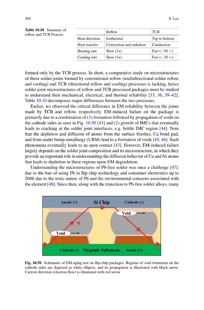
primarily due to a combination of (1) formation followed by propagation of voids on
the cathode sides as seen in Fig. 10.50 [43] and (2) growth of IMCs that eventually
leads to cracking at the solder joint interfaces, e.g. brittle IMC region [44]. Note
that the depletion and diffusion of atoms from the surface finishes, Cu bond pad,
and from under bump metallurgy (UBM) lead to a formation of voids [45, 46]. Such
phenomena eventually leads to an open contact [43]. However, EM-induced failure
largely depends on the solder joint composition and its microstructure, in which they
provide an important role in understanding the diffusion behavior of Cu and Ni atoms
that leads to depletion in these regions upon EM degradation.
Understanding the microstructures of Pb-free solder was once a challenge [47].
due to the ban of using Pb in flip-chip technology and consumer electronics up to
2006 due to the toxic nature of Pb and the environmental concerns associated with
the element [48]. Since then, along with the transition to Pb-free solder alloys, many
Fig. 10.50 Schematic of EM-aging test on flip-chip packages. Regions of void formation on the
cathode sides are depicted as white ellipses, and its propagation is illustrated with black arrow.
Current direction (electron flow) is illustrated with red arrow
S. Lee
Table 10.10 Summary of
reflow and TCB Process
Reflow
TCB
Heat direction
Isothermal
Top to bottom
Heat transfer
Convection and radiation
Conduction
Heating rate
Slow (1x)
Fast (~ 50 ×)
Cooling rate
Slow (1x)
Fast (~ 20 ×)
formed only by the TCB process. In short, a comparative study on microstructures
of these solder joints formed by conventional reflow (multidirectional solder reflow
and cooling) and TCB (directional reflow and cooling) processes is lacking, hence
solder joint microstructures of reflow and TCB processed packages must be studied
to understand their mechanical, electrical, and thermal reliability [33, 36, 39–42].
Table 10.10 decomposes major differences between the two processes.
Earlier, we observed the critical difference in EM reliability between the joints
made by TCB and reflow, respectively. EM-induced failure on the package is
primarily due to a combination of (1) formation followed by propagation of voids on
the cathode sides as seen in Fig. 10.50 [43] and (2) growth of IMCs that eventually
leads to cracking at the solder joint interfaces, e.g. brittle IMC region [44]. Note
that the depletion and diffusion of atoms from the surface finishes, Cu bond pad,
and from under bump metallurgy (UBM) lead to a formation of voids [45, 46]. Such
phenomena eventually leads to an open contact [43]. However, EM-induced failure
largely depends on the solder joint composition and its microstructure, in which they
provide an important role in understanding the diffusion behavior of Cu and Ni atoms
that leads to depletion in these regions upon EM degradation.
Understanding the microstructures of Pb-free solder was once a challenge [47].
due to the ban of using Pb in flip-chip technology and consumer electronics up to
2006 due to the toxic nature of Pb and the environmental concerns associated with
the element [48]. Since then, along with the transition to Pb-free solder alloys, many
Fig. 10.50 Schematic of EM-aging test on flip-chip packages. Regions of void formation on the
cathode sides are depicted as white ellipses, and its propagation is illustrated with black arrow.
Current direction (electron flow) is illustrated with red arrow