

300
S. Lee
Table 10.7 Configuration of
test vehicles
Die
Dimensions (mm)
10 × 12 × 0.2
Bump pitch (μm)
60/120
# of bumps
7744
Bump height (μm)
35
Interposer
Dimensions (mm)
27.05 × 19.25 × 0.1
Bump pitch (μm)
180
TSV dimensions (μm)
10 × 100
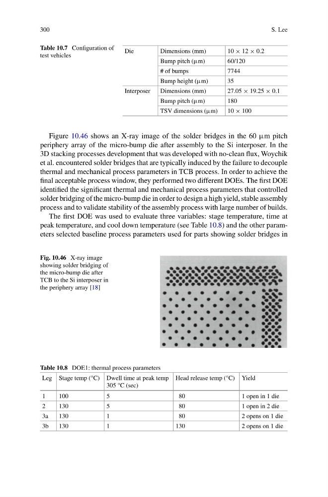
Figure 10.46 shows an X-ray image of the solder bridges in the 60 μm pitch
periphery array of the micro-bump die after assembly to the Si interposer. In the
3D stacking processes development that was developed with no-clean flux, Woychik
et al. encountered solder bridges that are typically induced by the failure to decouple
thermal and mechanical process parameters in TCB process. In order to achieve the
final acceptable process window, they performed two different DOEs. The first DOE
identified the significant thermal and mechanical process parameters that controlled
solder bridging of the micro-bump die in order to design a high yield, stable assembly
process and to validate stability of the assembly process with large number of builds.
The first DOE was used to evaluate three variables: stage temperature, time at
peak temperature, and cool down temperature (see Table 10.8) and the other parameters selected baseline process parameters used for parts showing solder bridges in
Fig. 10.46 X-ray image
showing solder bridging of
the micro-bump die after
TCB to the Si interposer in
the periphery array [18]
Table 10.8 DOE1: thermal process parameters
Leg Stage temp (°C) Dwell time at peak temp
305 °C (sec)
Head release temp (°C) Yield
1
100
5
80
1 open in 1 die
2
130
5
80
1 open in 2 die
3a
130
1
80
2 opens on 1 die
3b
130
1
130
2 opens on 1 die
S. Lee
Table 10.7 Configuration of
test vehicles
Die
Dimensions (mm)
10 × 12 × 0.2
Bump pitch (μm)
60/120
# of bumps
7744
Bump height (μm)
35
Interposer
Dimensions (mm)
27.05 × 19.25 × 0.1
Bump pitch (μm)
180
TSV dimensions (μm)
10 × 100
Figure 10.46 shows an X-ray image of the solder bridges in the 60 μm pitch
periphery array of the micro-bump die after assembly to the Si interposer. In the
3D stacking processes development that was developed with no-clean flux, Woychik
et al. encountered solder bridges that are typically induced by the failure to decouple
thermal and mechanical process parameters in TCB process. In order to achieve the
final acceptable process window, they performed two different DOEs. The first DOE
identified the significant thermal and mechanical process parameters that controlled
solder bridging of the micro-bump die in order to design a high yield, stable assembly
process and to validate stability of the assembly process with large number of builds.
The first DOE was used to evaluate three variables: stage temperature, time at
peak temperature, and cool down temperature (see Table 10.8) and the other parameters selected baseline process parameters used for parts showing solder bridges in
Fig. 10.46 X-ray image
showing solder bridging of
the micro-bump die after
TCB to the Si interposer in
the periphery array [18]
Table 10.8 DOE1: thermal process parameters
Leg Stage temp (°C) Dwell time at peak temp
305 °C (sec)
Head release temp (°C) Yield
1
100
5
80
1 open in 1 die
2
130
5
80
1 open in 2 die
3a
130
1
80
2 opens on 1 die
3b
130
1
130
2 opens on 1 die