

224
T. Suga et al.
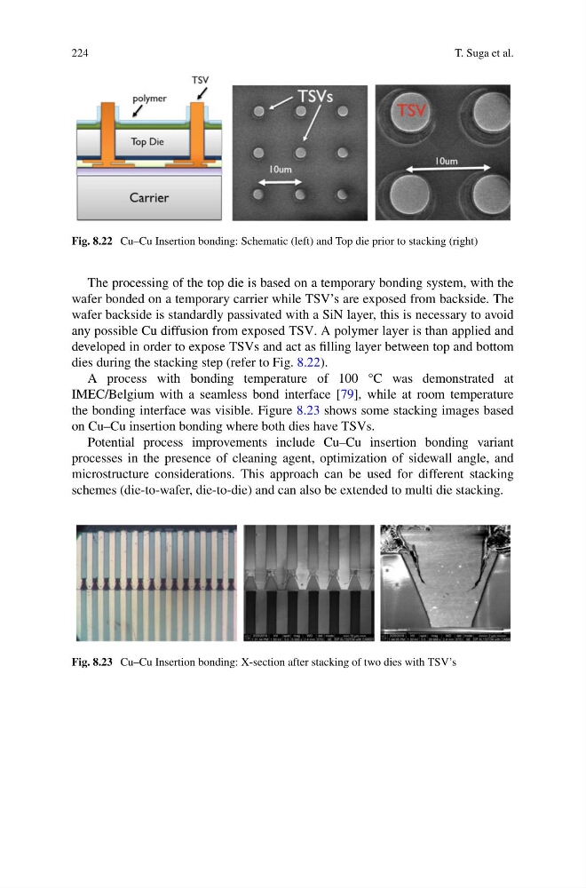
Fig. 8.22 Cu–Cu Insertion bonding: Schematic (left) and Top die prior to stacking (right)
The processing of the top die is based on a temporary bonding system, with the
wafer bonded on a temporary carrier while TSV’s are exposed from backside. The
wafer backside is standardly passivated with a SiN layer, this is necessary to avoid
any possible Cu diffusion from exposed TSV. A polymer layer is than applied and
developed in order to expose TSVs and act as filling layer between top and bottom
dies during the stacking step (refer to Fig. 8.22).
A process with bonding temperature of 100 °C was demonstrated at
IMEC/Belgium with a seamless bond interface [79], while at room temperature
the bonding interface was visible. Figure 8.23 shows some stacking images based
on Cu–Cu insertion bonding where both dies have TSVs.
Potential process improvements include Cu–Cu insertion bonding variant
processes in the presence of cleaning agent, optimization of sidewall angle, and
microstructure considerations. This approach can be used for different stacking
schemes (die-to-wafer, die-to-die) and can also be extended to multi die stacking.
Fig. 8.23 Cu–Cu Insertion bonding: X-section after stacking of two dies with TSV’s
T. Suga et al.
Fig. 8.22 Cu–Cu Insertion bonding: Schematic (left) and Top die prior to stacking (right)
The processing of the top die is based on a temporary bonding system, with the
wafer bonded on a temporary carrier while TSV’s are exposed from backside. The
wafer backside is standardly passivated with a SiN layer, this is necessary to avoid
any possible Cu diffusion from exposed TSV. A polymer layer is than applied and
developed in order to expose TSVs and act as filling layer between top and bottom
dies during the stacking step (refer to Fig. 8.22).
A process with bonding temperature of 100 °C was demonstrated at
IMEC/Belgium with a seamless bond interface [79], while at room temperature
the bonding interface was visible. Figure 8.23 shows some stacking images based
on Cu–Cu insertion bonding where both dies have TSVs.
Potential process improvements include Cu–Cu insertion bonding variant
processes in the presence of cleaning agent, optimization of sidewall angle, and
microstructure considerations. This approach can be used for different stacking
schemes (die-to-wafer, die-to-die) and can also be extended to multi die stacking.
Fig. 8.23 Cu–Cu Insertion bonding: X-section after stacking of two dies with TSV’s