

212
T. Suga et al.
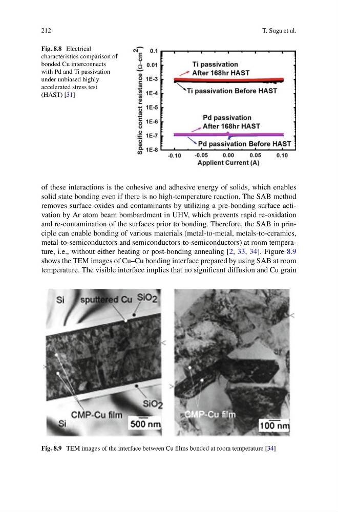
Fig. 8.8 Electrical
characteristics comparison of
bonded Cu interconnects
with Pd and Ti passivation
under unbiased highly
accelerated stress test
(HAST) [31]
of these interactions is the cohesive and adhesive energy of solids, which enables
solid state bonding even if there is no high-temperature reaction. The SAB method
removes surface oxides and contaminants by utilizing a pre-bonding surface activation by Ar atom beam bombardment in UHV, which prevents rapid re-oxidation
and re-contamination of the surfaces prior to bonding. Therefore, the SAB in principle can enable bonding of various materials (metal-to-metal, metals-to-ceramics,
metal-to-semiconductors and semiconductors-to-semiconductors) at room temperature, i.e., without either heating or post-bonding annealing [2, 33, 34]. Figure 8.9
shows the TEM images of Cu–Cu bonding interface prepared by using SAB at room
temperature. The visible interface implies that no significant diffusion and Cu grain
Fig. 8.9 TEM images of the interface between Cu films bonded at room temperature [34]
T. Suga et al.
Fig. 8.8 Electrical
characteristics comparison of
bonded Cu interconnects
with Pd and Ti passivation
under unbiased highly
accelerated stress test
(HAST) [31]
of these interactions is the cohesive and adhesive energy of solids, which enables
solid state bonding even if there is no high-temperature reaction. The SAB method
removes surface oxides and contaminants by utilizing a pre-bonding surface activation by Ar atom beam bombardment in UHV, which prevents rapid re-oxidation
and re-contamination of the surfaces prior to bonding. Therefore, the SAB in principle can enable bonding of various materials (metal-to-metal, metals-to-ceramics,
metal-to-semiconductors and semiconductors-to-semiconductors) at room temperature, i.e., without either heating or post-bonding annealing [2, 33, 34]. Figure 8.9
shows the TEM images of Cu–Cu bonding interface prepared by using SAB at room
temperature. The visible interface implies that no significant diffusion and Cu grain
Fig. 8.9 TEM images of the interface between Cu films bonded at room temperature [34]