

8 Direct Cu to Cu Bonding and Alternative Bonding Techniques …
205
Insulation/wiring
(a)
Si
Active layer
Si
Active layer
Active layer
Thinned Si
Active layer
Si
Active layer
Active layer
Thinned Si
Active layer
Insulation/wiring
Insulation/wiring
Thinned Si
Active layer
Si
Active layer
Active layer
B2F
Si
Active layer
B2F
Si
Active layer
Backside thinning and processing
for subsequent bonding
(b)
(c)
w/ or w/o TSVs
F2F
Temporary bonded
carrier
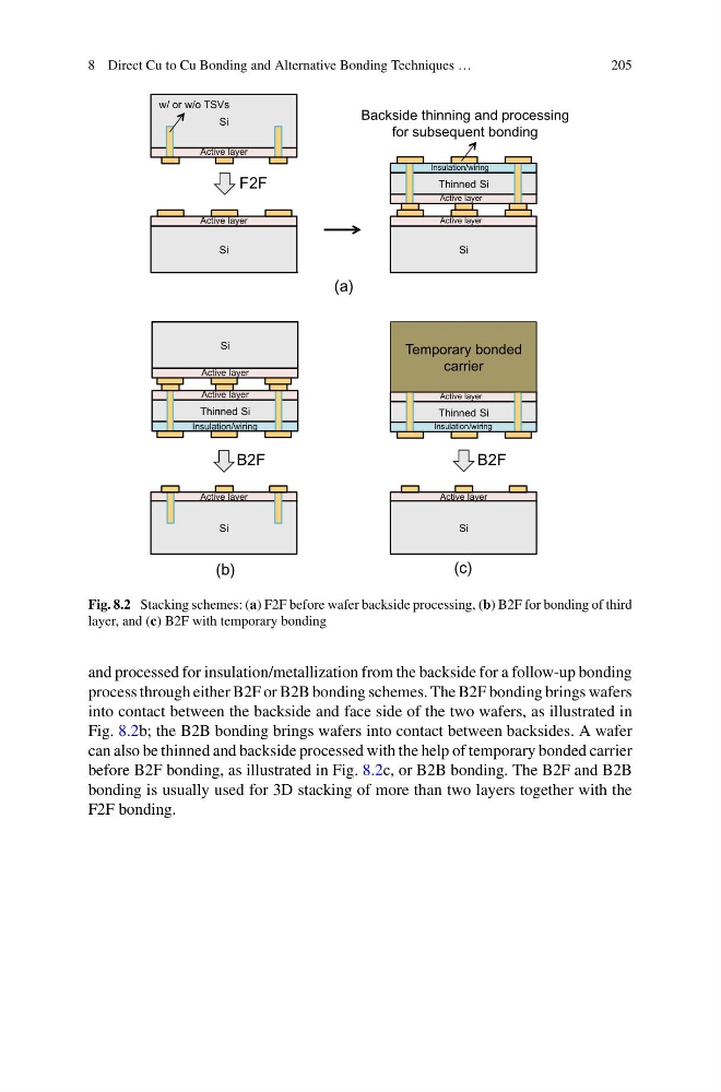
Fig. 8.2 Stacking schemes: (a) F2F before wafer backside processing, (b) B2F for bonding of third
layer, and (c) B2F with temporary bonding
and processed for insulation/metallization from the backside for a follow-up bonding
process through either B2F or B2B bonding schemes. The B2F bonding brings wafers
into contact between the backside and face side of the two wafers, as illustrated in
Fig. 8.2b; the B2B bonding brings wafers into contact between backsides. A wafer
can also be thinned and backside processed with the help of temporary bonded carrier
before B2F bonding, as illustrated in Fig. 8.2c, or B2B bonding. The B2F and B2B
bonding is usually used for 3D stacking of more than two layers together with the
F2F bonding.
205
Insulation/wiring
(a)
Si
Active layer
Si
Active layer
Active layer
Thinned Si
Active layer
Si
Active layer
Active layer
Thinned Si
Active layer
Insulation/wiring
Insulation/wiring
Thinned Si
Active layer
Si
Active layer
Active layer
B2F
Si
Active layer
B2F
Si
Active layer
Backside thinning and processing
for subsequent bonding
(b)
(c)
w/ or w/o TSVs
F2F
Temporary bonded
carrier
Fig. 8.2 Stacking schemes: (a) F2F before wafer backside processing, (b) B2F for bonding of third
layer, and (c) B2F with temporary bonding
and processed for insulation/metallization from the backside for a follow-up bonding
process through either B2F or B2B bonding schemes. The B2F bonding brings wafers
into contact between the backside and face side of the two wafers, as illustrated in
Fig. 8.2b; the B2B bonding brings wafers into contact between backsides. A wafer
can also be thinned and backside processed with the help of temporary bonded carrier
before B2F bonding, as illustrated in Fig. 8.2c, or B2B bonding. The B2F and B2B
bonding is usually used for 3D stacking of more than two layers together with the
F2F bonding.