

166
H. Ma et al.
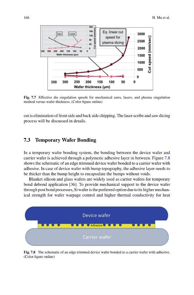
Fig. 7.7 Effective die singulation speeds for mechanical saws, lasers, and plasma singulation
method versus wafer thickness. (Color figure online)
cut is elimination of front side and back side chipping. The laser scribe and saw dicing
process will be discussed in details.
7.3 Temporary Wafer Bonding
In a temporary wafer bonding system, the bonding between the device wafer and
carrier wafer is achieved through a polymeric adhesive layer in between. Figure 7.8
shows the schematic of an edge trimmed device wafer bonded to a carrier wafer with
adhesive. In case of device wafer with bump topography, the adhesive layer needs to
be thicker than the bump height to encapsulate the bumps without voids.
Blanket silicon and glass wafers are widely used as carrier wafers for temporary
bond debond application [36]. To provide mechanical support to the device wafer
through post bond processes, Si wafer is the preferred option due to its higher mechanical strength for wafer warpage control and higher thermal conductivity for heat
Fig. 7.8 The schematic of an edge trimmed device wafer bonded to a carrier wafer with adhesive.
(Color figure online)
H. Ma et al.
Fig. 7.7 Effective die singulation speeds for mechanical saws, lasers, and plasma singulation
method versus wafer thickness. (Color figure online)
cut is elimination of front side and back side chipping. The laser scribe and saw dicing
process will be discussed in details.
7.3 Temporary Wafer Bonding
In a temporary wafer bonding system, the bonding between the device wafer and
carrier wafer is achieved through a polymeric adhesive layer in between. Figure 7.8
shows the schematic of an edge trimmed device wafer bonded to a carrier wafer with
adhesive. In case of device wafer with bump topography, the adhesive layer needs to
be thicker than the bump height to encapsulate the bumps without voids.
Blanket silicon and glass wafers are widely used as carrier wafers for temporary
bond debond application [36]. To provide mechanical support to the device wafer
through post bond processes, Si wafer is the preferred option due to its higher mechanical strength for wafer warpage control and higher thermal conductivity for heat
Fig. 7.8 The schematic of an edge trimmed device wafer bonded to a carrier wafer with adhesive.
(Color figure online)