

7 Fundamentals and Failures in Die Preparation for 3D Packaging
165
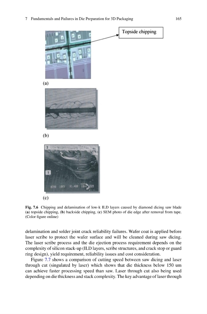
Fig. 7.6 Chipping and delamination of low-k ILD layers caused by diamond dicing saw blade
(a) topside chipping, (b) backside chipping, (c) SEM photo of die edge after removal from tape.
(Color figure online)
delamination and solder joint crack reliability failures. Wafer coat is applied before
laser scribe to protect the wafer surface and will be cleaned during saw dicing.
The laser scribe process and the die ejection process requirement depends on the
complexity of silicon stack-up (ILD layers, scribe structures, and crack stop or guard
ring design), yield requirement, reliability issues and cost consideration.
Figure 7.7 shows a comparison of cutting speed between saw dicing and laser
through cut (singulated by laser) which shows that die thickness below 150 um
can achieve faster processing speed than saw. Laser through cut also being used
depending on die thickness and stack complexity. The key advantage of laser through
165
Fig. 7.6 Chipping and delamination of low-k ILD layers caused by diamond dicing saw blade
(a) topside chipping, (b) backside chipping, (c) SEM photo of die edge after removal from tape.
(Color figure online)
delamination and solder joint crack reliability failures. Wafer coat is applied before
laser scribe to protect the wafer surface and will be cleaned during saw dicing.
The laser scribe process and the die ejection process requirement depends on the
complexity of silicon stack-up (ILD layers, scribe structures, and crack stop or guard
ring design), yield requirement, reliability issues and cost consideration.
Figure 7.7 shows a comparison of cutting speed between saw dicing and laser
through cut (singulated by laser) which shows that die thickness below 150 um
can achieve faster processing speed than saw. Laser through cut also being used
depending on die thickness and stack complexity. The key advantage of laser through