

160
H. Ma et al.
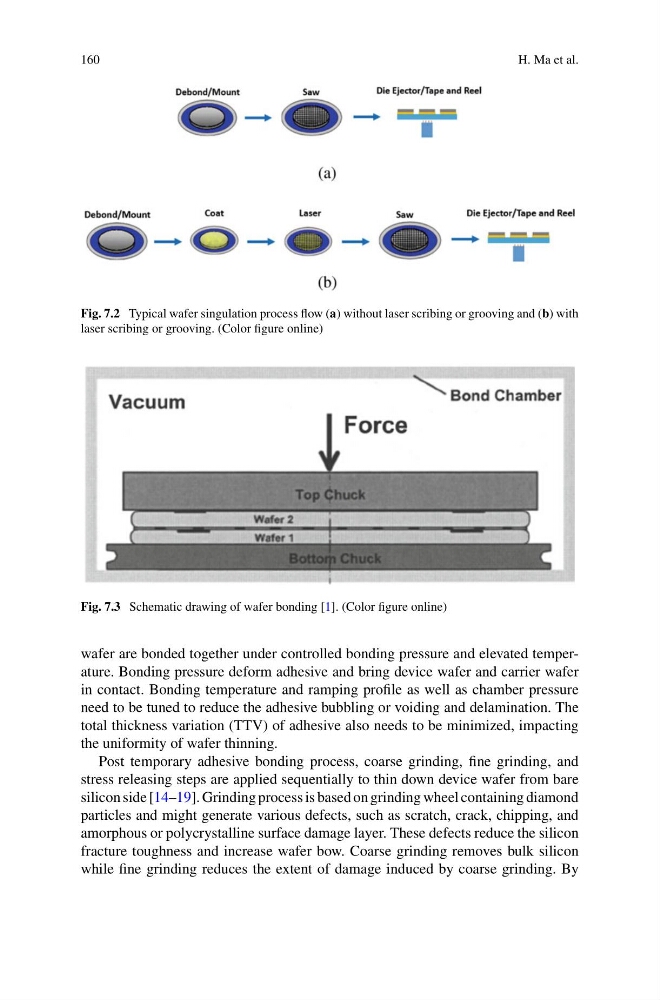
Fig. 7.2 Typical wafer singulation process flow (a) without laser scribing or grooving and (b) with
laser scribing or grooving. (Color figure online)
Fig. 7.3 Schematic drawing of wafer bonding [1]. (Color figure online)
wafer are bonded together under controlled bonding pressure and elevated temperature. Bonding pressure deform adhesive and bring device wafer and carrier wafer
in contact. Bonding temperature and ramping profile as well as chamber pressure
need to be tuned to reduce the adhesive bubbling or voiding and delamination. The
total thickness variation (TTV) of adhesive also needs to be minimized, impacting
the uniformity of wafer thinning.
Post temporary adhesive bonding process, coarse grinding, fine grinding, and
stress releasing steps are applied sequentially to thin down device wafer from bare
silicon side [14–19]. Grinding process is based on grinding wheel containing diamond
particles and might generate various defects, such as scratch, crack, chipping, and
amorphous or polycrystalline surface damage layer. These defects reduce the silicon
fracture toughness and increase wafer bow. Coarse grinding removes bulk silicon
while fine grinding reduces the extent of damage induced by coarse grinding. By
H. Ma et al.
Fig. 7.2 Typical wafer singulation process flow (a) without laser scribing or grooving and (b) with
laser scribing or grooving. (Color figure online)
Fig. 7.3 Schematic drawing of wafer bonding [1]. (Color figure online)
wafer are bonded together under controlled bonding pressure and elevated temperature. Bonding pressure deform adhesive and bring device wafer and carrier wafer
in contact. Bonding temperature and ramping profile as well as chamber pressure
need to be tuned to reduce the adhesive bubbling or voiding and delamination. The
total thickness variation (TTV) of adhesive also needs to be minimized, impacting
the uniformity of wafer thinning.
Post temporary adhesive bonding process, coarse grinding, fine grinding, and
stress releasing steps are applied sequentially to thin down device wafer from bare
silicon side [14–19]. Grinding process is based on grinding wheel containing diamond
particles and might generate various defects, such as scratch, crack, chipping, and
amorphous or polycrystalline surface damage layer. These defects reduce the silicon
fracture toughness and increase wafer bow. Coarse grinding removes bulk silicon
while fine grinding reduces the extent of damage induced by coarse grinding. By