

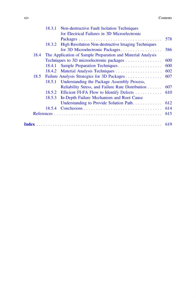
18.3.1 Non-destructive Fault Isolation Techniques
for Electrical Failures in 3D Microelectronic
Packages . . . . . . . . . . . . . . . . . . . . . . . . . . . . . . . . . . 578
18.3.2 High Resolution Non-destructive Imaging Techniques
for 3D Microelectronic Packages . . . . . . . . . . . . . . . . . 586
18.4 The Application of Sample Preparation and Material Analysis
Techniques to 3D microelectronic packages . . . . . . . . . . . . . . . 600
18.4.1 Sample Preparation Techniques . . . . . . . . . . . . . . . . . . 600
18.4.2 Material Analysis Techniques . . . . . . . . . . . . . . . . . . . 602
18.5 Failure Analysis Strategies for 3D Packages . . . . . . . . . . . . . . . 607
18.5.1 Understanding the Package Assembly Process,
Reliability Stress, and Failure Rate Distribution . . . . . . 607
18.5.2 Efficient FI-FA Flow to Identify Defects . . . . . . . . . . . 610
18.5.3 In-Depth Failure Mechanism and Root Cause
Understanding to Provide Solution Path . . . . . . . . . . . . 612
18.5.4 Conclusions . . . . . . . . . . . . . . . . . . . . . . . . . . . . . . . . 614
References . . . . . . . . . . . . . . . . . . . . . . . . . . . . . . . . . . . . . . . . . . . . 615
Index . . . . . . . . . . . . . . . . . . . . . . . . . . . . . . . . . . . . . . . . . . . . . . . . . . . . . . 619
xiv
Contents
for Electrical Failures in 3D Microelectronic
Packages . . . . . . . . . . . . . . . . . . . . . . . . . . . . . . . . . . 578
18.3.2 High Resolution Non-destructive Imaging Techniques
for 3D Microelectronic Packages . . . . . . . . . . . . . . . . . 586
18.4 The Application of Sample Preparation and Material Analysis
Techniques to 3D microelectronic packages . . . . . . . . . . . . . . . 600
18.4.1 Sample Preparation Techniques . . . . . . . . . . . . . . . . . . 600
18.4.2 Material Analysis Techniques . . . . . . . . . . . . . . . . . . . 602
18.5 Failure Analysis Strategies for 3D Packages . . . . . . . . . . . . . . . 607
18.5.1 Understanding the Package Assembly Process,
Reliability Stress, and Failure Rate Distribution . . . . . . 607
18.5.2 Efficient FI-FA Flow to Identify Defects . . . . . . . . . . . 610
18.5.3 In-Depth Failure Mechanism and Root Cause
Understanding to Provide Solution Path . . . . . . . . . . . . 612
18.5.4 Conclusions . . . . . . . . . . . . . . . . . . . . . . . . . . . . . . . . 614
References . . . . . . . . . . . . . . . . . . . . . . . . . . . . . . . . . . . . . . . . . . . . 615
Index . . . . . . . . . . . . . . . . . . . . . . . . . . . . . . . . . . . . . . . . . . . . . . . . . . . . . . 619
xiv
Contents