

564
M. Saini et al.
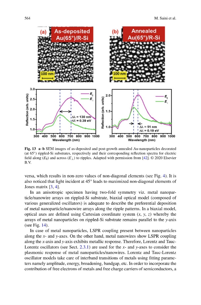
Fig. 13 a–b SEM images of as-deposited and post-growth annealed Au-nanoparticles decorated
(at 65°) rippled-Si substrates, respectively and their corresponding reflection spectra for electric
field along (E || ) and across (E ⊥ ) to ripples. Adapted with permission from [42]. © 2020 Elsevier
B.V.
versa, which results in non-zero values of non-diagonal elements (see Fig. 4). It is
also noticed that light incident at 45° leads to maximized non-diagonal elements of
Jones matrix [3, 4].
In an anisotropic specimen having two-fold symmetry viz. metal nanoparticle/nanowire arrays on rippled-Si substrate, biaxial optical model (composed of
various generalized oscillators) is adequate to describe the preferential deposition
of metal nanoparticle/nanowire arrays along the ripple patterns. In a biaxial model,
optical axes are defined using Cartesian coordinate system (x, y, z) whereby the
arrays of metal nanoparticles on rippled-Si substrate remains parallel to the y-axis
(see Fig. 14).
In case of metal nanoparticles, LSPR coupling present between nanoparticles
along the x- and y-axes. On the other hand, metal nanowires show LSPR coupling
along the x-axis and y-axis exhibits metallic response. Therefore, Lorentz and TaucLorentz oscillators (see Sect. 2.3.1) are used for the x- and y-axes to consider the
plasmonic response of metal nanoparticles/nanowires. Lorentz and Tauc-Lorentz
oscillator models take care of interband transitions of metals using fitting parameters namely amplitude, energy, broadening, bandgap, etc. In order to incorporate the
contribution of free electrons of metals and free charge carriers of semiconductors, a
M. Saini et al.
Fig. 13 a–b SEM images of as-deposited and post-growth annealed Au-nanoparticles decorated
(at 65°) rippled-Si substrates, respectively and their corresponding reflection spectra for electric
field along (E || ) and across (E ⊥ ) to ripples. Adapted with permission from [42]. © 2020 Elsevier
B.V.
versa, which results in non-zero values of non-diagonal elements (see Fig. 4). It is
also noticed that light incident at 45° leads to maximized non-diagonal elements of
Jones matrix [3, 4].
In an anisotropic specimen having two-fold symmetry viz. metal nanoparticle/nanowire arrays on rippled-Si substrate, biaxial optical model (composed of
various generalized oscillators) is adequate to describe the preferential deposition
of metal nanoparticle/nanowire arrays along the ripple patterns. In a biaxial model,
optical axes are defined using Cartesian coordinate system (x, y, z) whereby the
arrays of metal nanoparticles on rippled-Si substrate remains parallel to the y-axis
(see Fig. 14).
In case of metal nanoparticles, LSPR coupling present between nanoparticles
along the x- and y-axes. On the other hand, metal nanowires show LSPR coupling
along the x-axis and y-axis exhibits metallic response. Therefore, Lorentz and TaucLorentz oscillators (see Sect. 2.3.1) are used for the x- and y-axes to consider the
plasmonic response of metal nanoparticles/nanowires. Lorentz and Tauc-Lorentz
oscillator models take care of interband transitions of metals using fitting parameters namely amplitude, energy, broadening, bandgap, etc. In order to incorporate the
contribution of free electrons of metals and free charge carriers of semiconductors, a