

Fundamentals and Applications of Surface Enhanced Raman …
205
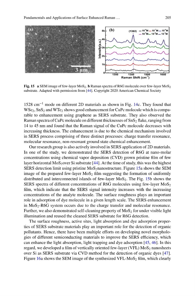
Fig. 15 a SEM image of few-layer MoS 2 . b Raman spectra of R6G molecule over few-layer MoS 2
substrate. Adapted with permission from [44]. Copyright 2020 American Chemical Society
1528 cm
−1 mode on different 2D materials as shown in Fig. 14c. They found that
WSe 2 , SnS 2 and WTe 2 shows good enhancement for CuPc molecule which is comparable to enhancement using graphene as SERS substrate. They also observed the
Raman spectra of CuPc molecule on different thicknesses of SnS 2 flake, ranging from
14 to 45 nm and found that the Raman signal of the CuPc molecule decreases with
increasing thickness. The enhancement is due to the chemical mechanism involved
in SERS process comprising of three distinct processes: charge transfer resonance,
molecular resonance, non-resonant ground state chemical enhancement.
Our research group is also actively involved in SERS application of 2D materials.
In one of the study, we demonstrated the SERS detection of R6G at nano-molar
concentrations using chemical vapor deposition (CVD) grown pristine film of few
layer horizontal MoS 2 over Si substrate [44]. At the time of study, this was the highest
SERS detection limit using pristine MoS 2 nanostructure. Figure 15a shows the SEM
image of the prepared few-layer MoS 2 film suggesting the formation of uniformly
distributed and interconnected islands of few-layer MoS 2 . The Fig. 15b shows the
SERS spectra of different concentrations of R6G molecules using few-layer MoS 2
film, which indicate that the SERS signal intensity increases with the increasing
concentrations of the analyte molecule. The surface roughness plays an important
role in adsorption of dye molecule in a given length scale. The SERS enhancement
in MoS 2 -R6G system occurs due to the charge transfer and molecular resonance.
Further, we also demonstrated self-cleaning property of MoS 2 for under visible light
illumination and reused the cleaned SERS substrate for R6G detection.
The surface roughness, active sites, light absorption and dye adsorption properties of SERS substrate materials play an important role for the detection of organic
pollutants. Hence, there have been multiple efforts on developing novel morphologies of different semiconducting materials to improve the SERS efficiency, which
can enhance the light absorption, light trapping and dye adsorption [45, 46]. In this
regard, we developed a film of vertically oriented few-layer (VFL) MoS 2 nanosheets
over Si as SERS substrate via CVD method for the detection of organic dyes [47].
Figure 16a shows the SEM image of the synthesized VFL-MoS 2 film, which clearly
205
Fig. 15 a SEM image of few-layer MoS 2 . b Raman spectra of R6G molecule over few-layer MoS 2
substrate. Adapted with permission from [44]. Copyright 2020 American Chemical Society
1528 cm
−1 mode on different 2D materials as shown in Fig. 14c. They found that
WSe 2 , SnS 2 and WTe 2 shows good enhancement for CuPc molecule which is comparable to enhancement using graphene as SERS substrate. They also observed the
Raman spectra of CuPc molecule on different thicknesses of SnS 2 flake, ranging from
14 to 45 nm and found that the Raman signal of the CuPc molecule decreases with
increasing thickness. The enhancement is due to the chemical mechanism involved
in SERS process comprising of three distinct processes: charge transfer resonance,
molecular resonance, non-resonant ground state chemical enhancement.
Our research group is also actively involved in SERS application of 2D materials.
In one of the study, we demonstrated the SERS detection of R6G at nano-molar
concentrations using chemical vapor deposition (CVD) grown pristine film of few
layer horizontal MoS 2 over Si substrate [44]. At the time of study, this was the highest
SERS detection limit using pristine MoS 2 nanostructure. Figure 15a shows the SEM
image of the prepared few-layer MoS 2 film suggesting the formation of uniformly
distributed and interconnected islands of few-layer MoS 2 . The Fig. 15b shows the
SERS spectra of different concentrations of R6G molecules using few-layer MoS 2
film, which indicate that the SERS signal intensity increases with the increasing
concentrations of the analyte molecule. The surface roughness plays an important
role in adsorption of dye molecule in a given length scale. The SERS enhancement
in MoS 2 -R6G system occurs due to the charge transfer and molecular resonance.
Further, we also demonstrated self-cleaning property of MoS 2 for under visible light
illumination and reused the cleaned SERS substrate for R6G detection.
The surface roughness, active sites, light absorption and dye adsorption properties of SERS substrate materials play an important role for the detection of organic
pollutants. Hence, there have been multiple efforts on developing novel morphologies of different semiconducting materials to improve the SERS efficiency, which
can enhance the light absorption, light trapping and dye adsorption [45, 46]. In this
regard, we developed a film of vertically oriented few-layer (VFL) MoS 2 nanosheets
over Si as SERS substrate via CVD method for the detection of organic dyes [47].
Figure 16a shows the SEM image of the synthesized VFL-MoS 2 film, which clearly