

Spin Transfer Torque Magnetoresistive Random Access Memory
91
RIE
IBE Trim
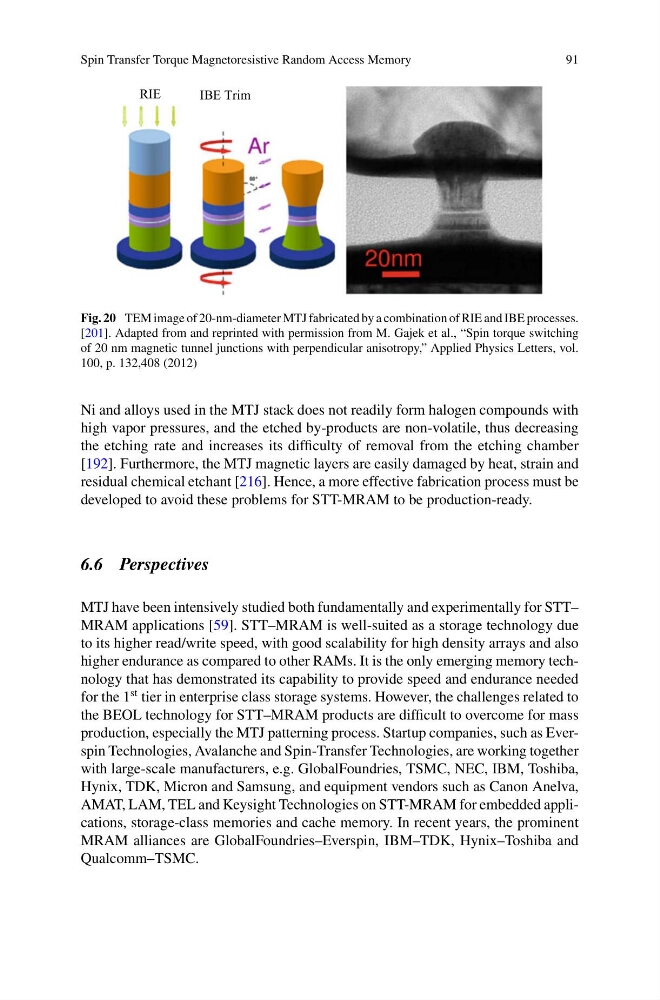
Fig. 20 TEM image of 20-nm-diameter MTJ fabricated by a combination of RIE and IBE processes.
[201]. Adapted from and reprinted with permission from M. Gajek et al., “Spin torque switching
of 20 nm magnetic tunnel junctions with perpendicular anisotropy,” Applied Physics Letters, vol.
100, p. 132,408 (2012)
Ni and alloys used in the MTJ stack does not readily form halogen compounds with
high vapor pressures, and the etched by-products are non-volatile, thus decreasing
the etching rate and increases its difficulty of removal from the etching chamber
[192]. Furthermore, the MTJ magnetic layers are easily damaged by heat, strain and
residual chemical etchant [216]. Hence, a more effective fabrication process must be
developed to avoid these problems for STT-MRAM to be production-ready.
6.6 Perspectives
MTJ have been intensively studied both fundamentally and experimentally for STT–
MRAM applications [59]. STT–MRAM is well-suited as a storage technology due
to its higher read/write speed, with good scalability for high density arrays and also
higher endurance as compared to other RAMs. It is the only emerging memory technology that has demonstrated its capability to provide speed and endurance needed
for the 1
st tier in enterprise class storage systems. However, the challenges related to
the BEOL technology for STT–MRAM products are difficult to overcome for mass
production, especially the MTJ patterning process. Startup companies, such as Everspin Technologies, Avalanche and Spin-Transfer Technologies, are working together
with large-scale manufacturers, e.g. GlobalFoundries, TSMC, NEC, IBM, Toshiba,
Hynix, TDK, Micron and Samsung, and equipment vendors such as Canon Anelva,
AMAT, LAM, TEL and Keysight Technologies on STT-MRAM for embedded applications, storage-class memories and cache memory. In recent years, the prominent
MRAM alliances are GlobalFoundries–Everspin, IBM–TDK, Hynix–Toshiba and
Qualcomm–TSMC.
91
RIE
IBE Trim
Fig. 20 TEM image of 20-nm-diameter MTJ fabricated by a combination of RIE and IBE processes.
[201]. Adapted from and reprinted with permission from M. Gajek et al., “Spin torque switching
of 20 nm magnetic tunnel junctions with perpendicular anisotropy,” Applied Physics Letters, vol.
100, p. 132,408 (2012)
Ni and alloys used in the MTJ stack does not readily form halogen compounds with
high vapor pressures, and the etched by-products are non-volatile, thus decreasing
the etching rate and increases its difficulty of removal from the etching chamber
[192]. Furthermore, the MTJ magnetic layers are easily damaged by heat, strain and
residual chemical etchant [216]. Hence, a more effective fabrication process must be
developed to avoid these problems for STT-MRAM to be production-ready.
6.6 Perspectives
MTJ have been intensively studied both fundamentally and experimentally for STT–
MRAM applications [59]. STT–MRAM is well-suited as a storage technology due
to its higher read/write speed, with good scalability for high density arrays and also
higher endurance as compared to other RAMs. It is the only emerging memory technology that has demonstrated its capability to provide speed and endurance needed
for the 1
st tier in enterprise class storage systems. However, the challenges related to
the BEOL technology for STT–MRAM products are difficult to overcome for mass
production, especially the MTJ patterning process. Startup companies, such as Everspin Technologies, Avalanche and Spin-Transfer Technologies, are working together
with large-scale manufacturers, e.g. GlobalFoundries, TSMC, NEC, IBM, Toshiba,
Hynix, TDK, Micron and Samsung, and equipment vendors such as Canon Anelva,
AMAT, LAM, TEL and Keysight Technologies on STT-MRAM for embedded applications, storage-class memories and cache memory. In recent years, the prominent
MRAM alliances are GlobalFoundries–Everspin, IBM–TDK, Hynix–Toshiba and
Qualcomm–TSMC.