

396
P. A. Dananjaya et al.
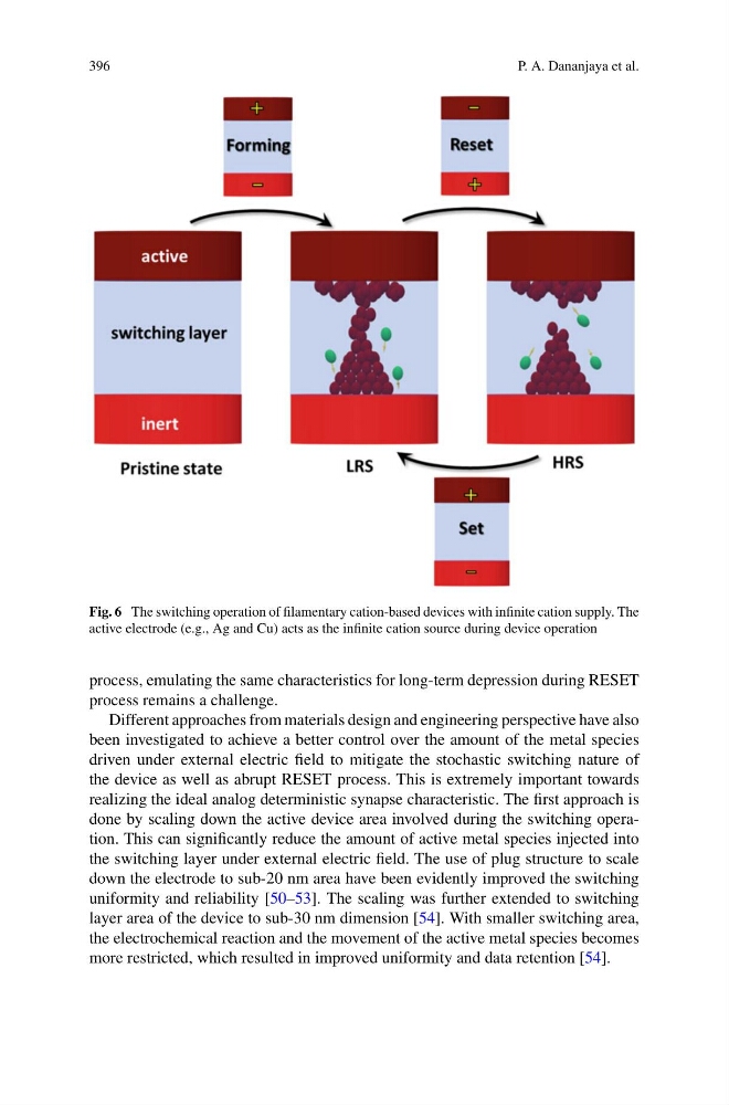
Fig. 6 The switching operation of filamentary cation-based devices with infinite cation supply. The
active electrode (e.g., Ag and Cu) acts as the infinite cation source during device operation
process, emulating the same characteristics for long-term depression during RESET
process remains a challenge.
Different approaches from materials design and engineering perspective have also
been investigated to achieve a better control over the amount of the metal species
driven under external electric field to mitigate the stochastic switching nature of
the device as well as abrupt RESET process. This is extremely important towards
realizing the ideal analog deterministic synapse characteristic. The first approach is
done by scaling down the active device area involved during the switching operation. This can significantly reduce the amount of active metal species injected into
the switching layer under external electric field. The use of plug structure to scale
down the electrode to sub-20 nm area have been evidently improved the switching
uniformity and reliability [50–53]. The scaling was further extended to switching
layer area of the device to sub-30 nm dimension [54]. With smaller switching area,
the electrochemical reaction and the movement of the active metal species becomes
more restricted, which resulted in improved uniformity and data retention [54].
P. A. Dananjaya et al.
Fig. 6 The switching operation of filamentary cation-based devices with infinite cation supply. The
active electrode (e.g., Ag and Cu) acts as the infinite cation source during device operation
process, emulating the same characteristics for long-term depression during RESET
process remains a challenge.
Different approaches from materials design and engineering perspective have also
been investigated to achieve a better control over the amount of the metal species
driven under external electric field to mitigate the stochastic switching nature of
the device as well as abrupt RESET process. This is extremely important towards
realizing the ideal analog deterministic synapse characteristic. The first approach is
done by scaling down the active device area involved during the switching operation. This can significantly reduce the amount of active metal species injected into
the switching layer under external electric field. The use of plug structure to scale
down the electrode to sub-20 nm area have been evidently improved the switching
uniformity and reliability [50–53]. The scaling was further extended to switching
layer area of the device to sub-30 nm dimension [54]. With smaller switching area,
the electrochemical reaction and the movement of the active metal species becomes
more restricted, which resulted in improved uniformity and data retention [54].