

RRAM Device Characterizations and Modelling
369
process, so the SET voltage will increase with the initial gap distance × 0 and HRS
as shown in Fig. 22a. Two different operation schemes are used to switch the device
from ~10 to ~50 k as shown in Fig. 22b. It implies that the switching speed will
exponentially increase with operation voltage during the RESET process. By tuning
parts of the parameters used in the model, the electrical characteristics of different
RRAM device with different material and structures can be reproduced [22]. Excellent agreement between the modelled and measured data in different RRAM devices
indicates the validity and universality of the developed compact model to describe
the main features of the bipolar RRAM cell operations.
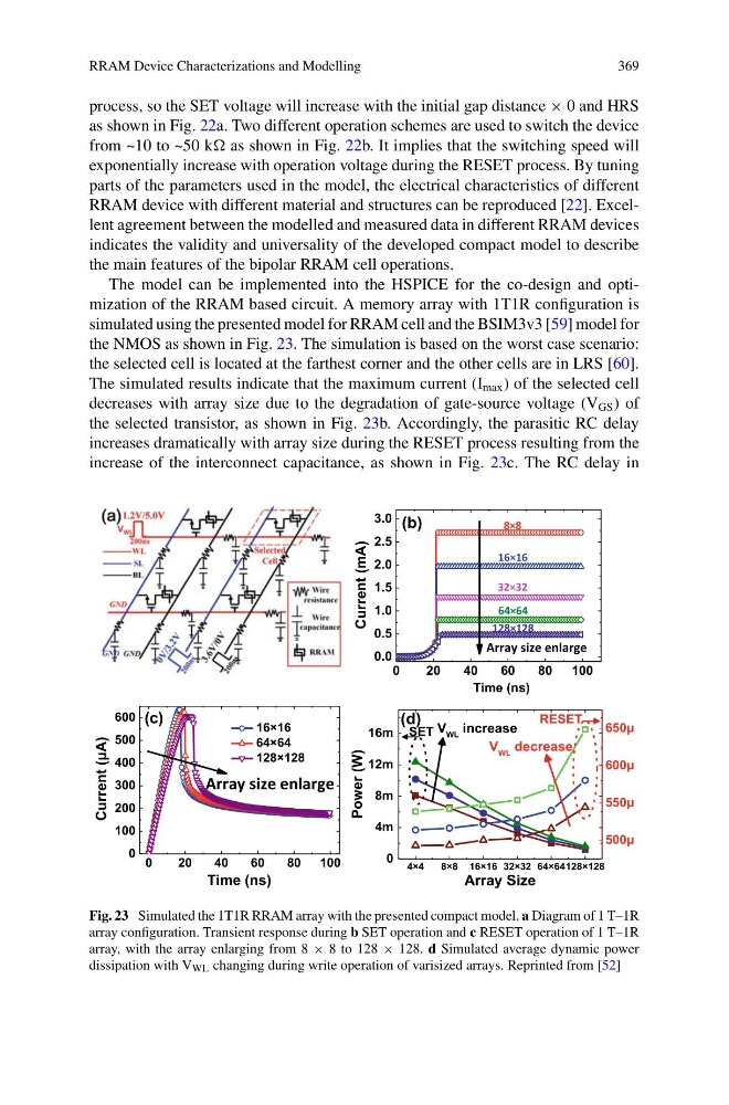
The model can be implemented into the HSPICE for the co-design and optimization of the RRAM based circuit. A memory array with 1T1R configuration is
simulated using the presented model for RRAM cell and the BSIM3v3 [59] model for
the NMOS as shown in Fig. 23. The simulation is based on the worst case scenario:
the selected cell is located at the farthest corner and the other cells are in LRS [60].
The simulated results indicate that the maximum current (I max ) of the selected cell
decreases with array size due to the degradation of gate-source voltage (V GS ) of
the selected transistor, as shown in Fig. 23b. Accordingly, the parasitic RC delay
increases dramatically with array size during the RESET process resulting from the
increase of the interconnect capacitance, as shown in Fig. 23c. The RC delay in
0
20
40
60
80
100
0.0
0.5
1.0
1.5
2.0
2.5
3.0
128×128
64×64
32×32
16×16
8×8
Current (mA)
Time (ns)
Array size enlarge
(b)
0
20
40
60
80
100
0
100
200
300
400
500
600
Current (μA)
Time (ns)
16×16
64×64
128×128
Array size enlarge
(c)
4×4
8×8 16×16 32×32 64×64128×128
0
4m
8m
12m
16m
Power (W)
Array Size
(d)
500μ
550μ
600μ
650μ
V WL decrease
SET
RESET
V WL increase
Fig. 23 Simulated the 1T1R RRAM array with the presented compact model. a Diagram of 1 T–1R
array configuration. Transient response during b SET operation and c RESET operation of 1 T–1R
array, with the array enlarging from 8 × 8 to 128 × 128. d Simulated average dynamic power
dissipation with V WL changing during write operation of varisized arrays. Reprinted from [52]
369
process, so the SET voltage will increase with the initial gap distance × 0 and HRS
as shown in Fig. 22a. Two different operation schemes are used to switch the device
from ~10 to ~50 k as shown in Fig. 22b. It implies that the switching speed will
exponentially increase with operation voltage during the RESET process. By tuning
parts of the parameters used in the model, the electrical characteristics of different
RRAM device with different material and structures can be reproduced [22]. Excellent agreement between the modelled and measured data in different RRAM devices
indicates the validity and universality of the developed compact model to describe
the main features of the bipolar RRAM cell operations.
The model can be implemented into the HSPICE for the co-design and optimization of the RRAM based circuit. A memory array with 1T1R configuration is
simulated using the presented model for RRAM cell and the BSIM3v3 [59] model for
the NMOS as shown in Fig. 23. The simulation is based on the worst case scenario:
the selected cell is located at the farthest corner and the other cells are in LRS [60].
The simulated results indicate that the maximum current (I max ) of the selected cell
decreases with array size due to the degradation of gate-source voltage (V GS ) of
the selected transistor, as shown in Fig. 23b. Accordingly, the parasitic RC delay
increases dramatically with array size during the RESET process resulting from the
increase of the interconnect capacitance, as shown in Fig. 23c. The RC delay in
0
20
40
60
80
100
0.0
0.5
1.0
1.5
2.0
2.5
3.0
128×128
64×64
32×32
16×16
8×8
Current (mA)
Time (ns)
Array size enlarge
(b)
0
20
40
60
80
100
0
100
200
300
400
500
600
Current (μA)
Time (ns)
16×16
64×64
128×128
Array size enlarge
(c)
4×4
8×8 16×16 32×32 64×64128×128
0
4m
8m
12m
16m
Power (W)
Array Size
(d)
500μ
550μ
600μ
650μ
V WL decrease
SET
RESET
V WL increase
Fig. 23 Simulated the 1T1R RRAM array with the presented compact model. a Diagram of 1 T–1R
array configuration. Transient response during b SET operation and c RESET operation of 1 T–1R
array, with the array enlarging from 8 × 8 to 128 × 128. d Simulated average dynamic power
dissipation with V WL changing during write operation of varisized arrays. Reprinted from [52]