

346
P. Huang et al.
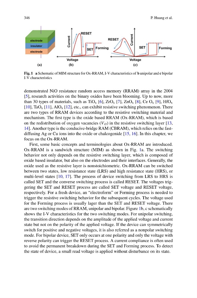
Fig. 1 a Schematic of MIM structure for Ox-RRAM, I-V characteristics of b unipolar and c bipolar
I-V characteristics
demonstrated NiO resistance random access memory (RRAM) array in the 2004
[5], research activities on the binary oxides have been blooming. Up to now, more
than 30 types of materials, such as TiO x [6], ZrO x [7], ZnO x [8], Ce O x [9], HfO x
[10], TaO x [11], AlO x [12], etc., can exhibit resistive switching phenomenon. There
are two types of RRAM devices according to the resistive switching material and
mechanism. The first type is the oxide based RRAM (Ox-RRAM), which is based
on the redistribution of oxygen vacancies (V O ) in the resistive switching layer [13,
14]. Another type is the conducive-bridge RAM (CBRAM), which relies on the fastdiffusing Ag or Cu ions into the oxide or chalcogenide [15, 16]. In this chapter, we
focus on the Ox-RRAM.
First, some basic concepts and terminologies about Ox-RRAM are introduced.
Ox-RRAM is a sandwich structure (MIM) as shown in Fig. 1a. The switching
behavior not only depends on the resistive switching layer, which is composed of
oxide based insulator, but also on the electrodes and their interfaces. Generally, the
oxide used as the resistive layer is nonstoichiometric. Ox-RRAM can be switched
between two states, low resistance state (LRS) and high resistance state (HRS), or
multi-level states [10, 17]. The process of device switching from LRS to HRS is
called SET and the converse switching process is called RESET. The voltages triggering the SET and RESET process are called SET voltage and RESET voltage,
respectively. For a fresh device, an “electroform” or Forming process is needed to
trigger the resistive switching behavior for the subsequent cycles. The voltage used
for the Forming process is usually lager than the SET and RESET voltage. There
are two switching modes of RRAM, unipolar and bipolar. Figure 1b, c schematically
shows the I-V characteristics for the two switching modes. For unipolar switching,
the transition direction depends on the amplitude of the applied voltage and current
state but not on the polarity of the applied voltage. If the device can symmetrically
switch for positive and negative voltages, it is also referred as a nonpolar switching
mode. For bipolar device, SET only occurs at one polarity and only the voltage with
reverse polarity can trigger the RESET process. A current compliance is often used
to avoid the permanent breakdown during the SET and Forming process. To detect
the state of device, a small read voltage is applied without disturbance on its state.
P. Huang et al.
Fig. 1 a Schematic of MIM structure for Ox-RRAM, I-V characteristics of b unipolar and c bipolar
I-V characteristics
demonstrated NiO resistance random access memory (RRAM) array in the 2004
[5], research activities on the binary oxides have been blooming. Up to now, more
than 30 types of materials, such as TiO x [6], ZrO x [7], ZnO x [8], Ce O x [9], HfO x
[10], TaO x [11], AlO x [12], etc., can exhibit resistive switching phenomenon. There
are two types of RRAM devices according to the resistive switching material and
mechanism. The first type is the oxide based RRAM (Ox-RRAM), which is based
on the redistribution of oxygen vacancies (V O ) in the resistive switching layer [13,
14]. Another type is the conducive-bridge RAM (CBRAM), which relies on the fastdiffusing Ag or Cu ions into the oxide or chalcogenide [15, 16]. In this chapter, we
focus on the Ox-RRAM.
First, some basic concepts and terminologies about Ox-RRAM are introduced.
Ox-RRAM is a sandwich structure (MIM) as shown in Fig. 1a. The switching
behavior not only depends on the resistive switching layer, which is composed of
oxide based insulator, but also on the electrodes and their interfaces. Generally, the
oxide used as the resistive layer is nonstoichiometric. Ox-RRAM can be switched
between two states, low resistance state (LRS) and high resistance state (HRS), or
multi-level states [10, 17]. The process of device switching from LRS to HRS is
called SET and the converse switching process is called RESET. The voltages triggering the SET and RESET process are called SET voltage and RESET voltage,
respectively. For a fresh device, an “electroform” or Forming process is needed to
trigger the resistive switching behavior for the subsequent cycles. The voltage used
for the Forming process is usually lager than the SET and RESET voltage. There
are two switching modes of RRAM, unipolar and bipolar. Figure 1b, c schematically
shows the I-V characteristics for the two switching modes. For unipolar switching,
the transition direction depends on the amplitude of the applied voltage and current
state but not on the polarity of the applied voltage. If the device can symmetrically
switch for positive and negative voltages, it is also referred as a nonpolar switching
mode. For bipolar device, SET only occurs at one polarity and only the voltage with
reverse polarity can trigger the RESET process. A current compliance is often used
to avoid the permanent breakdown during the SET and Forming process. To detect
the state of device, a small read voltage is applied without disturbance on its state.