

3D Nanomagnetic Logic
263
-2e-3
-1e-3
0
1e-3
2e-3
-200 -100
0
100 200
Areal Magnetization [emu/cm
2
]
Magnetic Induction [mT]
5 ML
10 ML
40 ML
2 m
µ
2 m
µ
2 m
µ
2 um
500 nm
Co/Pt, Co/Ni stack
SEM graph of a magnet array
Lithography + Ar ion etch
b
Define single−domain magnetic islands
10
5
40
Film deposition + characterization
Find prospective film composition
MFM graph of naturally formed film−domains
a
Control position of nucleation
’1’ ’0’
Control mean switching field
Energy
Ion irradiation
ANC−creation
c
M
H
FIB
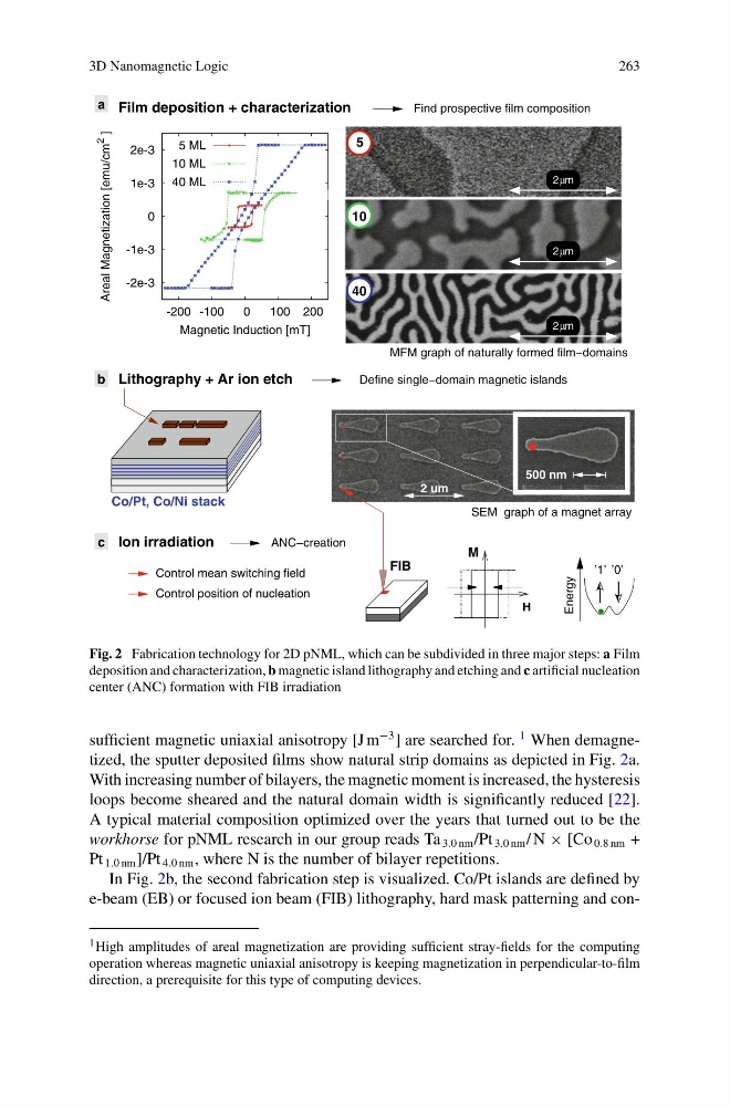
Fig. 2 Fabrication technology for 2D pNML, which can be subdivided in three major steps: a Film
deposition and characterization, b magnetic island lithography and etching and c artificial nucleation
center (ANC) formation with FIB irradiation
sufficient magnetic uniaxial anisotropy [J m
−3 ] are searched for.
1 When demagnetized, the sputter deposited films show natural strip domains as depicted in Fig. 2a.
With increasing number of bilayers, the magnetic moment is increased, the hysteresis
loops become sheared and the natural domain width is significantly reduced [22].
A typical material composition optimized over the years that turned out to be the
workhorse for pNML research in our group reads Ta 3.0 nm /Pt 3.0 nm / N × [Co 0.8 nm +
Pt 1.0 nm ]/Pt 4.0 nm , where N is the number of bilayer repetitions.
In Fig. 2b, the second fabrication step is visualized. Co/Pt islands are defined by
e-beam (EB) or focused ion beam (FIB) lithography, hard mask patterning and con1 High amplitudes of areal magnetization are providing sufficient stray-fields for the computing
operation whereas magnetic uniaxial anisotropy is keeping magnetization in perpendicular-to-film
direction, a prerequisite for this type of computing devices.
263
-2e-3
-1e-3
0
1e-3
2e-3
-200 -100
0
100 200
Areal Magnetization [emu/cm
2
]
Magnetic Induction [mT]
5 ML
10 ML
40 ML
2 m
µ
2 m
µ
2 m
µ
2 um
500 nm
Co/Pt, Co/Ni stack
SEM graph of a magnet array
Lithography + Ar ion etch
b
Define single−domain magnetic islands
10
5
40
Film deposition + characterization
Find prospective film composition
MFM graph of naturally formed film−domains
a
Control position of nucleation
’1’ ’0’
Control mean switching field
Energy
Ion irradiation
ANC−creation
c
M
H
FIB
Fig. 2 Fabrication technology for 2D pNML, which can be subdivided in three major steps: a Film
deposition and characterization, b magnetic island lithography and etching and c artificial nucleation
center (ANC) formation with FIB irradiation
sufficient magnetic uniaxial anisotropy [J m
−3 ] are searched for.
1 When demagnetized, the sputter deposited films show natural strip domains as depicted in Fig. 2a.
With increasing number of bilayers, the magnetic moment is increased, the hysteresis
loops become sheared and the natural domain width is significantly reduced [22].
A typical material composition optimized over the years that turned out to be the
workhorse for pNML research in our group reads Ta 3.0 nm /Pt 3.0 nm / N × [Co 0.8 nm +
Pt 1.0 nm ]/Pt 4.0 nm , where N is the number of bilayer repetitions.
In Fig. 2b, the second fabrication step is visualized. Co/Pt islands are defined by
e-beam (EB) or focused ion beam (FIB) lithography, hard mask patterning and con1 High amplitudes of areal magnetization are providing sufficient stray-fields for the computing
operation whereas magnetic uniaxial anisotropy is keeping magnetization in perpendicular-to-film
direction, a prerequisite for this type of computing devices.