

Domain Wall Programmable Magnetic Logic
247
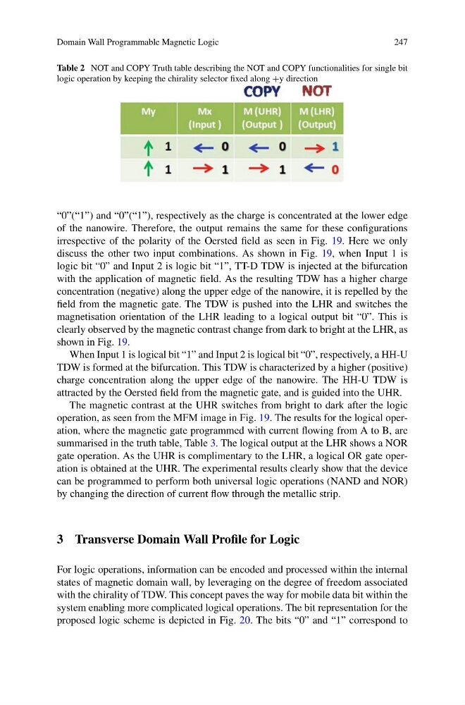
Table 2 NOT and COPY Truth table describing the NOT and COPY functionalities for single bit
logic operation by keeping the chirality selector fixed along +y direction
“0”(“1”) and “0”(“1”), respectively as the charge is concentrated at the lower edge
of the nanowire. Therefore, the output remains the same for these configurations
irrespective of the polarity of the Oersted field as seen in Fig. 19. Here we only
discuss the other two input combinations. As shown in Fig. 19, when Input 1 is
logic bit “0” and Input 2 is logic bit “1”, TT-D TDW is injected at the bifurcation
with the application of magnetic field. As the resulting TDW has a higher charge
concentration (negative) along the upper edge of the nanowire, it is repelled by the
field from the magnetic gate. The TDW is pushed into the LHR and switches the
magnetisation orientation of the LHR leading to a logical output bit “0”. This is
clearly observed by the magnetic contrast change from dark to bright at the LHR, as
shown in Fig. 19.
When Input 1 is logical bit “1” and Input 2 is logical bit “0”, respectively, a HH-U
TDW is formed at the bifurcation. This TDW is characterized by a higher (positive)
charge concentration along the upper edge of the nanowire. The HH-U TDW is
attracted by the Oersted field from the magnetic gate, and is guided into the UHR.
The magnetic contrast at the UHR switches from bright to dark after the logic
operation, as seen from the MFM image in Fig. 19. The results for the logical operation, where the magnetic gate programmed with current flowing from A to B, are
summarised in the truth table, Table 3. The logical output at the LHR shows a NOR
gate operation. As the UHR is complimentary to the LHR, a logical OR gate operation is obtained at the UHR. The experimental results clearly show that the device
can be programmed to perform both universal logic operations (NAND and NOR)
by changing the direction of current flow through the metallic strip.
3 Transverse Domain Wall Profile for Logic
For logic operations, information can be encoded and processed within the internal
states of magnetic domain wall, by leveraging on the degree of freedom associated
with the chirality of TDW. This concept paves the way for mobile data bit within the
system enabling more complicated logical operations. The bit representation for the
proposed logic scheme is depicted in Fig. 20. The bits “0” and “1” correspond to
247
Table 2 NOT and COPY Truth table describing the NOT and COPY functionalities for single bit
logic operation by keeping the chirality selector fixed along +y direction
“0”(“1”) and “0”(“1”), respectively as the charge is concentrated at the lower edge
of the nanowire. Therefore, the output remains the same for these configurations
irrespective of the polarity of the Oersted field as seen in Fig. 19. Here we only
discuss the other two input combinations. As shown in Fig. 19, when Input 1 is
logic bit “0” and Input 2 is logic bit “1”, TT-D TDW is injected at the bifurcation
with the application of magnetic field. As the resulting TDW has a higher charge
concentration (negative) along the upper edge of the nanowire, it is repelled by the
field from the magnetic gate. The TDW is pushed into the LHR and switches the
magnetisation orientation of the LHR leading to a logical output bit “0”. This is
clearly observed by the magnetic contrast change from dark to bright at the LHR, as
shown in Fig. 19.
When Input 1 is logical bit “1” and Input 2 is logical bit “0”, respectively, a HH-U
TDW is formed at the bifurcation. This TDW is characterized by a higher (positive)
charge concentration along the upper edge of the nanowire. The HH-U TDW is
attracted by the Oersted field from the magnetic gate, and is guided into the UHR.
The magnetic contrast at the UHR switches from bright to dark after the logic
operation, as seen from the MFM image in Fig. 19. The results for the logical operation, where the magnetic gate programmed with current flowing from A to B, are
summarised in the truth table, Table 3. The logical output at the LHR shows a NOR
gate operation. As the UHR is complimentary to the LHR, a logical OR gate operation is obtained at the UHR. The experimental results clearly show that the device
can be programmed to perform both universal logic operations (NAND and NOR)
by changing the direction of current flow through the metallic strip.
3 Transverse Domain Wall Profile for Logic
For logic operations, information can be encoded and processed within the internal
states of magnetic domain wall, by leveraging on the degree of freedom associated
with the chirality of TDW. This concept paves the way for mobile data bit within the
system enabling more complicated logical operations. The bit representation for the
proposed logic scheme is depicted in Fig. 20. The bits “0” and “1” correspond to