

Domain Wall Programmable Magnetic Logic
243
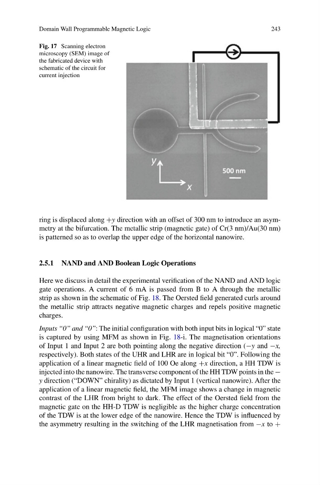
Fig. 17 Scanning electron
microscopy (SEM) image of
the fabricated device with
schematic of the circuit for
current injection
ring is displaced along +y direction with an offset of 300 nm to introduce an asymmetry at the bifurcation. The metallic strip (magnetic gate) of Cr(3 nm)/Au(30 nm)
is patterned so as to overlap the upper edge of the horizontal nanowire.
2.5.1 NAND and AND Boolean Logic Operations
Here we discuss in detail the experimental verification of the NAND and AND logic
gate operations. A current of 6 mA is passed from B to A through the metallic
strip as shown in the schematic of Fig. 18. The Oersted field generated curls around
the metallic strip attracts negative magnetic charges and repels positive magnetic
charges.
Inputs “0” and “0”: The initial configuration with both input bits in logical “0” state
is captured by using MFM as shown in Fig. 18-i. The magnetisation orientations
of Input 1 and Input 2 are both pointing along the negative direction (−y and −x,
respectively). Both states of the UHR and LHR are in logical bit “0”. Following the
application of a linear magnetic field of 100 Oe along +x direction, a HH TDW is
injected into the nanowire. The transverse component of the HH TDW points in the −
y direction (“DOWN” chirality) as dictated by Input 1 (vertical nanowire). After the
application of a linear magnetic field, the MFM image shows a change in magnetic
contrast of the LHR from bright to dark. The effect of the Oersted field from the
magnetic gate on the HH-D TDW is negligible as the higher charge concentration
of the TDW is at the lower edge of the nanowire. Hence the TDW is influenced by
the asymmetry resulting in the switching of the LHR magnetisation from −x to +
243
Fig. 17 Scanning electron
microscopy (SEM) image of
the fabricated device with
schematic of the circuit for
current injection
ring is displaced along +y direction with an offset of 300 nm to introduce an asymmetry at the bifurcation. The metallic strip (magnetic gate) of Cr(3 nm)/Au(30 nm)
is patterned so as to overlap the upper edge of the horizontal nanowire.
2.5.1 NAND and AND Boolean Logic Operations
Here we discuss in detail the experimental verification of the NAND and AND logic
gate operations. A current of 6 mA is passed from B to A through the metallic
strip as shown in the schematic of Fig. 18. The Oersted field generated curls around
the metallic strip attracts negative magnetic charges and repels positive magnetic
charges.
Inputs “0” and “0”: The initial configuration with both input bits in logical “0” state
is captured by using MFM as shown in Fig. 18-i. The magnetisation orientations
of Input 1 and Input 2 are both pointing along the negative direction (−y and −x,
respectively). Both states of the UHR and LHR are in logical bit “0”. Following the
application of a linear magnetic field of 100 Oe along +x direction, a HH TDW is
injected into the nanowire. The transverse component of the HH TDW points in the −
y direction (“DOWN” chirality) as dictated by Input 1 (vertical nanowire). After the
application of a linear magnetic field, the MFM image shows a change in magnetic
contrast of the LHR from bright to dark. The effect of the Oersted field from the
magnetic gate on the HH-D TDW is negligible as the higher charge concentration
of the TDW is at the lower edge of the nanowire. Hence the TDW is influenced by
the asymmetry resulting in the switching of the LHR magnetisation from −x to +