

204
T. T.-H. Kim
is explained followed by design challenges in magnetic memory. Then, various circuit
techniques for write and sensing for magnetic memory are discussed in the following
section.
2 Overview of Magnetic Memory Cells
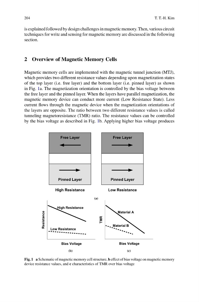
Magnetic memory cells are implemented with the magnetic tunnel junction (MTJ),
which provides two different resistance values depending upon magnetization states
of the top layer (i.e. free layer) and the bottom layer (i.e. pinned layer) as shown
in Fig. 1a. The magnetization orientation is controlled by the bias voltage between
the free layer and the pinned layer. When the layers have parallel magnetization, the
magnetic memory device can conduct more current (Low Resistance State). Less
current flows through the magnetic device when the magnetization orientations of
the layers are opposite. The ratio between two different resistance values is called
tunneling magnetoresistance (TMR) ratio. The resistance values can be controlled
by the bias voltage as described in Fig. 1b. Applying higher bias voltage produces
Free Layer
Pinned Layer
Free Layer
Pinned Layer
High Resistance
Low Resistance
(a)
Bias Voltage
TMR
Material A
Material B
Bias Voltage
Resistance
High Resistance
Low Resistance
(b)
(c)
Fig. 1 a Schematic of magnetic memory cell structure, b effect of bias voltage on magnetic memory
device resistance values, and c characteristics of TMR over bias voltage
T. T.-H. Kim
is explained followed by design challenges in magnetic memory. Then, various circuit
techniques for write and sensing for magnetic memory are discussed in the following
section.
2 Overview of Magnetic Memory Cells
Magnetic memory cells are implemented with the magnetic tunnel junction (MTJ),
which provides two different resistance values depending upon magnetization states
of the top layer (i.e. free layer) and the bottom layer (i.e. pinned layer) as shown
in Fig. 1a. The magnetization orientation is controlled by the bias voltage between
the free layer and the pinned layer. When the layers have parallel magnetization, the
magnetic memory device can conduct more current (Low Resistance State). Less
current flows through the magnetic device when the magnetization orientations of
the layers are opposite. The ratio between two different resistance values is called
tunneling magnetoresistance (TMR) ratio. The resistance values can be controlled
by the bias voltage as described in Fig. 1b. Applying higher bias voltage produces
Free Layer
Pinned Layer
Free Layer
Pinned Layer
High Resistance
Low Resistance
(a)
Bias Voltage
TMR
Material A
Material B
Bias Voltage
Resistance
High Resistance
Low Resistance
(b)
(c)
Fig. 1 a Schematic of magnetic memory cell structure, b effect of bias voltage on magnetic memory
device resistance values, and c characteristics of TMR over bias voltage