

158
J. Lourembam and J. Huang
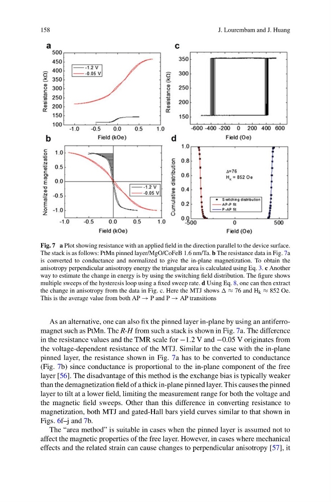
Fig. 7 a Plot showing resistance with an applied field in the direction parallel to the device surface.
The stack is as follows: PtMn pinned layer/MgO/CoFeB 1.6 nm/Ta. b The resistance data in Fig. 7a
is converted to conductance and normalized to give the in-plane magnetization. To obtain the
anisotropy perpendicular anisotropy energy the triangular area is calculated using Eq. 3. c Another
way to estimate the change in energy is by using the switching field distribution. The figure shows
multiple sweeps of the hysteresis loop using a fixed sweep rate. d Using Eq. 8, one can then extract
the change in anisotropy from the data in Fig. c. Here the MTJ shows ≈ 76 and H k ≈ 852 Oe.
This is the average value from both AP → P and P → AP transitions
As an alternative, one can also fix the pinned layer in-plane by using an antiferromagnet such as PtMn. The R-H from such a stack is shown in Fig. 7a. The difference
in the resistance values and the TMR scale for −1.2 V and −0.05 V originates from
the voltage-dependent resistance of the MTJ. Similar to the case with the in-plane
pinned layer, the resistance shown in Fig. 7a has to be converted to conductance
(Fig. 7b) since conductance is proportional to the in-plane component of the free
layer [56]. The disadvantage of this method is the exchange bias is typically weaker
than the demagnetization field of a thick in-plane pinned layer. This causes the pinned
layer to tilt at a lower field, limiting the measurement range for both the voltage and
the magnetic field sweeps. Other than this difference in converting resistance to
magnetization, both MTJ and gated-Hall bars yield curves similar to that shown in
Figs. 6f–j and 7b.
The “area method” is suitable in cases when the pinned layer is assumed not to
affect the magnetic properties of the free layer. However, in cases where mechanical
effects and the related strain can cause changes to perpendicular anisotropy [57], it
J. Lourembam and J. Huang
Fig. 7 a Plot showing resistance with an applied field in the direction parallel to the device surface.
The stack is as follows: PtMn pinned layer/MgO/CoFeB 1.6 nm/Ta. b The resistance data in Fig. 7a
is converted to conductance and normalized to give the in-plane magnetization. To obtain the
anisotropy perpendicular anisotropy energy the triangular area is calculated using Eq. 3. c Another
way to estimate the change in energy is by using the switching field distribution. The figure shows
multiple sweeps of the hysteresis loop using a fixed sweep rate. d Using Eq. 8, one can then extract
the change in anisotropy from the data in Fig. c. Here the MTJ shows ≈ 76 and H k ≈ 852 Oe.
This is the average value from both AP → P and P → AP transitions
As an alternative, one can also fix the pinned layer in-plane by using an antiferromagnet such as PtMn. The R-H from such a stack is shown in Fig. 7a. The difference
in the resistance values and the TMR scale for −1.2 V and −0.05 V originates from
the voltage-dependent resistance of the MTJ. Similar to the case with the in-plane
pinned layer, the resistance shown in Fig. 7a has to be converted to conductance
(Fig. 7b) since conductance is proportional to the in-plane component of the free
layer [56]. The disadvantage of this method is the exchange bias is typically weaker
than the demagnetization field of a thick in-plane pinned layer. This causes the pinned
layer to tilt at a lower field, limiting the measurement range for both the voltage and
the magnetic field sweeps. Other than this difference in converting resistance to
magnetization, both MTJ and gated-Hall bars yield curves similar to that shown in
Figs. 6f–j and 7b.
The “area method” is suitable in cases when the pinned layer is assumed not to
affect the magnetic properties of the free layer. However, in cases where mechanical
effects and the related strain can cause changes to perpendicular anisotropy [57], it