

selectivity owing to its nanoporous structure. The carriers formed from light irradiation migrate in the crystal through the wires. However, the wires may be randomly
broken in the crystal because of inherent defects, which form active centers for
molecular adsorption and redox reactions. To date, the influences of structural
defects in ETS-10 on the adsorption and reaction dynamics of organic compounds
have not been well characterized. The spatial heterogeneities of the surfaces and the
inhomogeneous coupling interface between the adsorbed molecules and the nanoscale rough surfaces of the semiconductor make the dissecting of the complex
interfacial ET processes highly difficult. The in situ fluorescence imaging of
photocatalytic oxidation was carried out on single ETS-10 crystals using a redoxresponsive fluorescent dye; 3
0 -( p-aminophenyl) fluorescein (APF), which was commonly used for the selective detection of
•
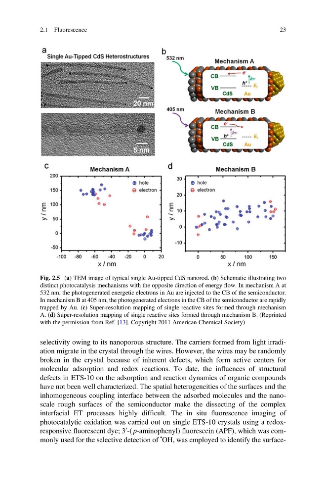
OH, was employed to identify the surfaceFig. 2.5 (a) TEM image of typical single Au-tipped CdS nanorod. (b) Schematic illustrating two
distinct photocatalysis mechanisms with the opposite direction of energy flow. In mechanism A at
532 nm, the photogenerated energetic electrons in Au are injected to the CB of the semiconductor.
In mechanism B at 405 nm, the photogenerated electrons in the CB of the semiconductor are rapidly
trapped by Au. (c) Super-resolution mapping of single reactive sites formed through mechanism
A. (d) Super-resolution mapping of single reactive sites formed through mechanism B. (Reprinted
with the permission from Ref. [13]. Copyright 2011 American Chemical Society)
2.1 Fluorescence
23
broken in the crystal because of inherent defects, which form active centers for
molecular adsorption and redox reactions. To date, the influences of structural
defects in ETS-10 on the adsorption and reaction dynamics of organic compounds
have not been well characterized. The spatial heterogeneities of the surfaces and the
inhomogeneous coupling interface between the adsorbed molecules and the nanoscale rough surfaces of the semiconductor make the dissecting of the complex
interfacial ET processes highly difficult. The in situ fluorescence imaging of
photocatalytic oxidation was carried out on single ETS-10 crystals using a redoxresponsive fluorescent dye; 3
0 -( p-aminophenyl) fluorescein (APF), which was commonly used for the selective detection of
•
OH, was employed to identify the surfaceFig. 2.5 (a) TEM image of typical single Au-tipped CdS nanorod. (b) Schematic illustrating two
distinct photocatalysis mechanisms with the opposite direction of energy flow. In mechanism A at
532 nm, the photogenerated energetic electrons in Au are injected to the CB of the semiconductor.
In mechanism B at 405 nm, the photogenerated electrons in the CB of the semiconductor are rapidly
trapped by Au. (c) Super-resolution mapping of single reactive sites formed through mechanism
A. (d) Super-resolution mapping of single reactive sites formed through mechanism B. (Reprinted
with the permission from Ref. [13]. Copyright 2011 American Chemical Society)
2.1 Fluorescence
23