

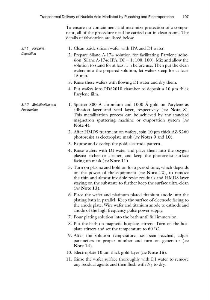
To ensure no containment and maximize protection of a component, all of the procedure need be carried out in clean room. The
details of fabrication are listed below.
3.1.1 Parylene
Deposition
1. Clean oxide silicon wafer with IPA and DI water.
2. Prepare Silane A-174 solution for facilitating Parylene adhesion (Silane A-174: IPA: DI ¼ 1: 100: 100). Mix and allow the
solution to stand for at least 1 h before use. Then put the clean
wafers into the prepared solution, let wafers steep for at least
15 min.
3. Rinse these wafers with flowing DI water and dry them.
4. Put wafers into PDS2010 chamber to deposit a 10 μm thick
Parylene film.
3.1.2 Metallization and
Electroplate
1. Sputter 300 A ˚ chromium and 1000 A ˚ gold on Parylene as
adhesion layer and seed layer, respectively (see Note 8).
This metallization process can be achieved by any standard
magnetron sputtering machine or evaporation system (see
Note 4).
2. After HMDS treatment on wafers, spin 10 μm thick AZ 9260
photoresist as electroplate mask (see Notes 9 and 10).
3. Expose and develop the gold electrode pattern.
4. Rinse wafers with DI water and place them into the oxygen
plasma etcher or cleaner, and keep the photoresist surface
facing up mask (see Note 11).
5. Turn on plasma and hold on for a period time, which depends
on the power of the equipment (see Note 12), to remove
the thin and almost invisible resist residuals and HMDS layer
staying on the substrate to further keep the surface ultra-clean
(see Note 13).
6. Place the wafer and platinum-plated titanium anode into the
plating bath in parallel. Keep the surface of electrode facing to
the anode plate. Wire wafer and titanium anode to cathode and
anode of the high frequency pulse power supply.
7. Pour plating solution into the bath until full immersion.
8. Put the bath on magnetic hotplate stirrers. Turn on the hotplate stirrers and set the temperature to 60
C.
9. After the solution temperature has been reached, adjust
parameters to proper number and turn on generator (see
Note 14).
10. Electroplate 10 μm thick gold layer (see Note 15).
11. Rinse the wafer surface thoroughly with DI water to remove
any residual agents and then flush with N 2 to dry.
Transdermal Delivery of Nucleic Acid Mediated by Punching and Electroporation
107
details of fabrication are listed below.
3.1.1 Parylene
Deposition
1. Clean oxide silicon wafer with IPA and DI water.
2. Prepare Silane A-174 solution for facilitating Parylene adhesion (Silane A-174: IPA: DI ¼ 1: 100: 100). Mix and allow the
solution to stand for at least 1 h before use. Then put the clean
wafers into the prepared solution, let wafers steep for at least
15 min.
3. Rinse these wafers with flowing DI water and dry them.
4. Put wafers into PDS2010 chamber to deposit a 10 μm thick
Parylene film.
3.1.2 Metallization and
Electroplate
1. Sputter 300 A ˚ chromium and 1000 A ˚ gold on Parylene as
adhesion layer and seed layer, respectively (see Note 8).
This metallization process can be achieved by any standard
magnetron sputtering machine or evaporation system (see
Note 4).
2. After HMDS treatment on wafers, spin 10 μm thick AZ 9260
photoresist as electroplate mask (see Notes 9 and 10).
3. Expose and develop the gold electrode pattern.
4. Rinse wafers with DI water and place them into the oxygen
plasma etcher or cleaner, and keep the photoresist surface
facing up mask (see Note 11).
5. Turn on plasma and hold on for a period time, which depends
on the power of the equipment (see Note 12), to remove
the thin and almost invisible resist residuals and HMDS layer
staying on the substrate to further keep the surface ultra-clean
(see Note 13).
6. Place the wafer and platinum-plated titanium anode into the
plating bath in parallel. Keep the surface of electrode facing to
the anode plate. Wire wafer and titanium anode to cathode and
anode of the high frequency pulse power supply.
7. Pour plating solution into the bath until full immersion.
8. Put the bath on magnetic hotplate stirrers. Turn on the hotplate stirrers and set the temperature to 60
C.
9. After the solution temperature has been reached, adjust
parameters to proper number and turn on generator (see
Note 14).
10. Electroplate 10 μm thick gold layer (see Note 15).
11. Rinse the wafer surface thoroughly with DI water to remove
any residual agents and then flush with N 2 to dry.
Transdermal Delivery of Nucleic Acid Mediated by Punching and Electroporation
107