

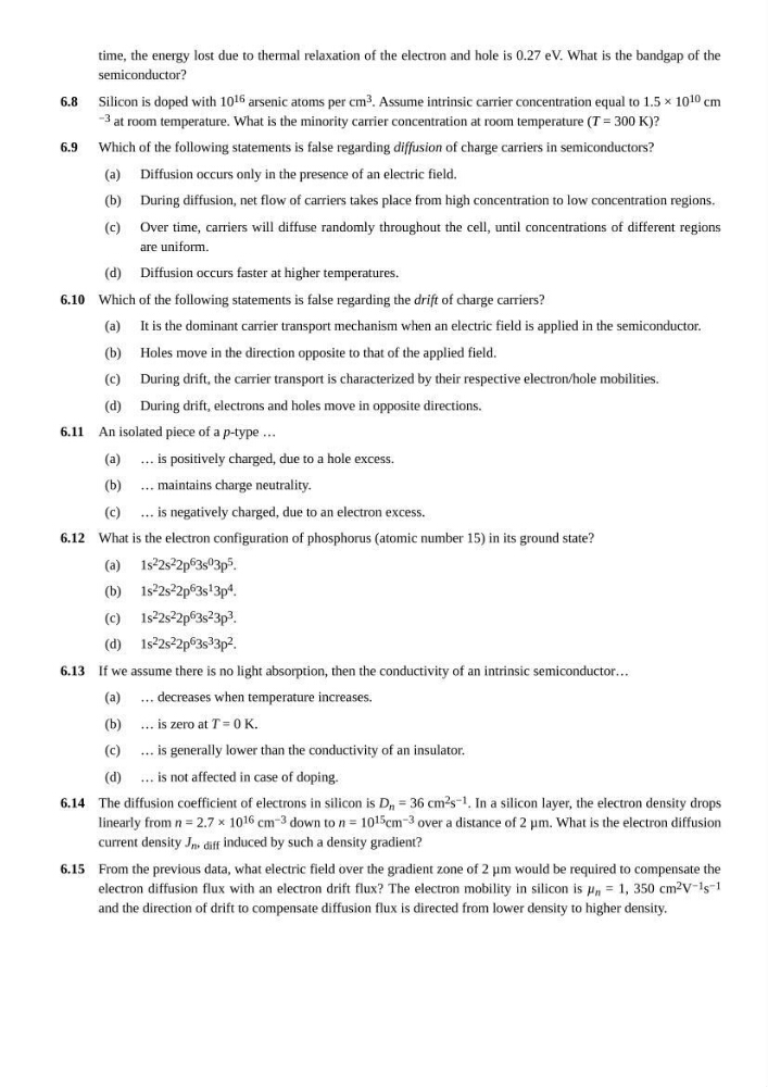
6.8
6.9
(a)
(b)
(c)
(d)
6.10
(a)
(b)
(c)
(d)
6.11
(a)
(b)
(c)
6.12
(a)
(b)
(c)
(d)
6.13
(a)
(b)
(c)
(d)
6.14
6.15
time, the energy lost due to thermal relaxation of the electron and hole is 0.27 eV. What is the bandgap of the
semiconductor?
Silicon is doped with 10 16 arsenic atoms per cm 3 . Assume intrinsic carrier concentration equal to 1.5 × 10 10 cm
−3 at room temperature. What is the minority carrier concentration at room temperature (T = 300 K)?
Which of the following statements is false regarding diffusion of charge carriers in semiconductors?
Diffusion occurs only in the presence of an electric field.
During diffusion, net flow of carriers takes place from high concentration to low concentration regions.
Over time, carriers will diffuse randomly throughout the cell, until concentrations of different regions
are uniform.
Diffusion occurs faster at higher temperatures.
Which of the following statements is false regarding the drift of charge carriers?
It is the dominant carrier transport mechanism when an electric field is applied in the semiconductor.
Holes move in the direction opposite to that of the applied field.
During drift, the carrier transport is characterized by their respective electron/hole mobilities.
During drift, electrons and holes move in opposite directions.
An isolated piece of a p-type …
… is positively charged, due to a hole excess.
… maintains charge neutrality.
… is negatively charged, due to an electron excess.
What is the electron configuration of phosphorus (atomic number 15) in its ground state?
1s 2 2s 2 2p 6 3s 0 3p 5 .
1s 2 2s 2 2p 6 3s 1 3p 4 .
1s 2 2s 2 2p 6 3s 2 3p 3 .
1s 2 2s 2 2p 6 3s 3 3p 2 .
If we assume there is no light absorption, then the conductivity of an intrinsic semiconductor…
… decreases when temperature increases.
… is zero at T = 0 K.
… is generally lower than the conductivity of an insulator.
… is not affected in case of doping.
The diffusion coefficient of electrons in silicon is D n = 36 cm 2 s −1 . In a silicon layer, the electron density drops
linearly from n = 2.7 × 10 16 cm −3 down to n = 10 15 cm −3 over a distance of 2 µm. What is the electron diffusion
current density J n , diff induced by such a density gradient?
From the previous data, what electric field over the gradient zone of 2 µm would be required to compensate the
electron diffusion flux with an electron drift flux? The electron mobility in silicon is µ n = 1, 350 cm 2 V −1 s −1
and the direction of drift to compensate diffusion flux is directed from lower density to higher density.
6.9
(a)
(b)
(c)
(d)
6.10
(a)
(b)
(c)
(d)
6.11
(a)
(b)
(c)
6.12
(a)
(b)
(c)
(d)
6.13
(a)
(b)
(c)
(d)
6.14
6.15
time, the energy lost due to thermal relaxation of the electron and hole is 0.27 eV. What is the bandgap of the
semiconductor?
Silicon is doped with 10 16 arsenic atoms per cm 3 . Assume intrinsic carrier concentration equal to 1.5 × 10 10 cm
−3 at room temperature. What is the minority carrier concentration at room temperature (T = 300 K)?
Which of the following statements is false regarding diffusion of charge carriers in semiconductors?
Diffusion occurs only in the presence of an electric field.
During diffusion, net flow of carriers takes place from high concentration to low concentration regions.
Over time, carriers will diffuse randomly throughout the cell, until concentrations of different regions
are uniform.
Diffusion occurs faster at higher temperatures.
Which of the following statements is false regarding the drift of charge carriers?
It is the dominant carrier transport mechanism when an electric field is applied in the semiconductor.
Holes move in the direction opposite to that of the applied field.
During drift, the carrier transport is characterized by their respective electron/hole mobilities.
During drift, electrons and holes move in opposite directions.
An isolated piece of a p-type …
… is positively charged, due to a hole excess.
… maintains charge neutrality.
… is negatively charged, due to an electron excess.
What is the electron configuration of phosphorus (atomic number 15) in its ground state?
1s 2 2s 2 2p 6 3s 0 3p 5 .
1s 2 2s 2 2p 6 3s 1 3p 4 .
1s 2 2s 2 2p 6 3s 2 3p 3 .
1s 2 2s 2 2p 6 3s 3 3p 2 .
If we assume there is no light absorption, then the conductivity of an intrinsic semiconductor…
… decreases when temperature increases.
… is zero at T = 0 K.
… is generally lower than the conductivity of an insulator.
… is not affected in case of doping.
The diffusion coefficient of electrons in silicon is D n = 36 cm 2 s −1 . In a silicon layer, the electron density drops
linearly from n = 2.7 × 10 16 cm −3 down to n = 10 15 cm −3 over a distance of 2 µm. What is the electron diffusion
current density J n , diff induced by such a density gradient?
From the previous data, what electric field over the gradient zone of 2 µm would be required to compensate the
electron diffusion flux with an electron drift flux? The electron mobility in silicon is µ n = 1, 350 cm 2 V −1 s −1
and the direction of drift to compensate diffusion flux is directed from lower density to higher density.