

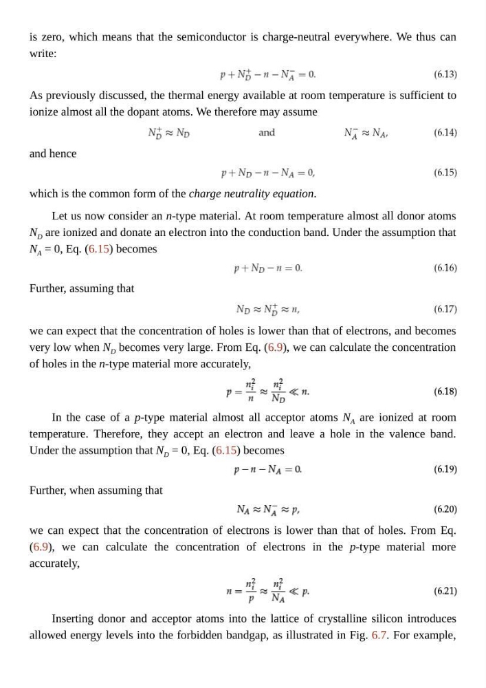
is zero, which means that the semiconductor is charge-neutral everywhere. We thus can
write:
As previously discussed, the thermal energy available at room temperature is sufficient to
ionize almost all the dopant atoms. We therefore may assume
and hence
which is the common form of the charge neutrality equation.
Let us now consider an n-type material. At room temperature almost all donor atoms
N D are ionized and donate an electron into the conduction band. Under the assumption that
N A = 0, Eq. (6.15) becomes
Further, assuming that
we can expect that the concentration of holes is lower than that of electrons, and becomes
very low when N D becomes very large. From Eq. (6.9), we can calculate the concentration
of holes in the n-type material more accurately,
In the case of a p-type material almost all acceptor atoms N A are ionized at room
temperature. Therefore, they accept an electron and leave a hole in the valence band.
Under the assumption that N D = 0, Eq. (6.15) becomes
Further, when assuming that
we can expect that the concentration of electrons is lower than that of holes. From Eq.
(6.9), we can calculate the concentration of electrons in the p-type material more
accurately,
Inserting donor and acceptor atoms into the lattice of crystalline silicon introduces
allowed energy levels into the forbidden bandgap, as illustrated in Fig. 6.7. For example,
write:
As previously discussed, the thermal energy available at room temperature is sufficient to
ionize almost all the dopant atoms. We therefore may assume
and hence
which is the common form of the charge neutrality equation.
Let us now consider an n-type material. At room temperature almost all donor atoms
N D are ionized and donate an electron into the conduction band. Under the assumption that
N A = 0, Eq. (6.15) becomes
Further, assuming that
we can expect that the concentration of holes is lower than that of electrons, and becomes
very low when N D becomes very large. From Eq. (6.9), we can calculate the concentration
of holes in the n-type material more accurately,
In the case of a p-type material almost all acceptor atoms N A are ionized at room
temperature. Therefore, they accept an electron and leave a hole in the valence band.
Under the assumption that N D = 0, Eq. (6.15) becomes
Further, when assuming that
we can expect that the concentration of electrons is lower than that of holes. From Eq.
(6.9), we can calculate the concentration of electrons in the p-type material more
accurately,
Inserting donor and acceptor atoms into the lattice of crystalline silicon introduces
allowed energy levels into the forbidden bandgap, as illustrated in Fig. 6.7. For example,