

polytechnique fédérale de Lausanne (EPFL), Switzerland [197], was prepared using lowpressure chemical vapour deposition (LP-CVD). Both materials obtain their nano structure
during the deposition process. The nano structures are due to the crystal growth of the
TCO layers and have a pyramid-like shape.
In contrast, RF-sputtered, aluminium-doped zinc oxide (ZnO:Al) is flat after
deposition (σ r ≈ 3 nm, depending on the deposition condition). To obtain a nano texture,
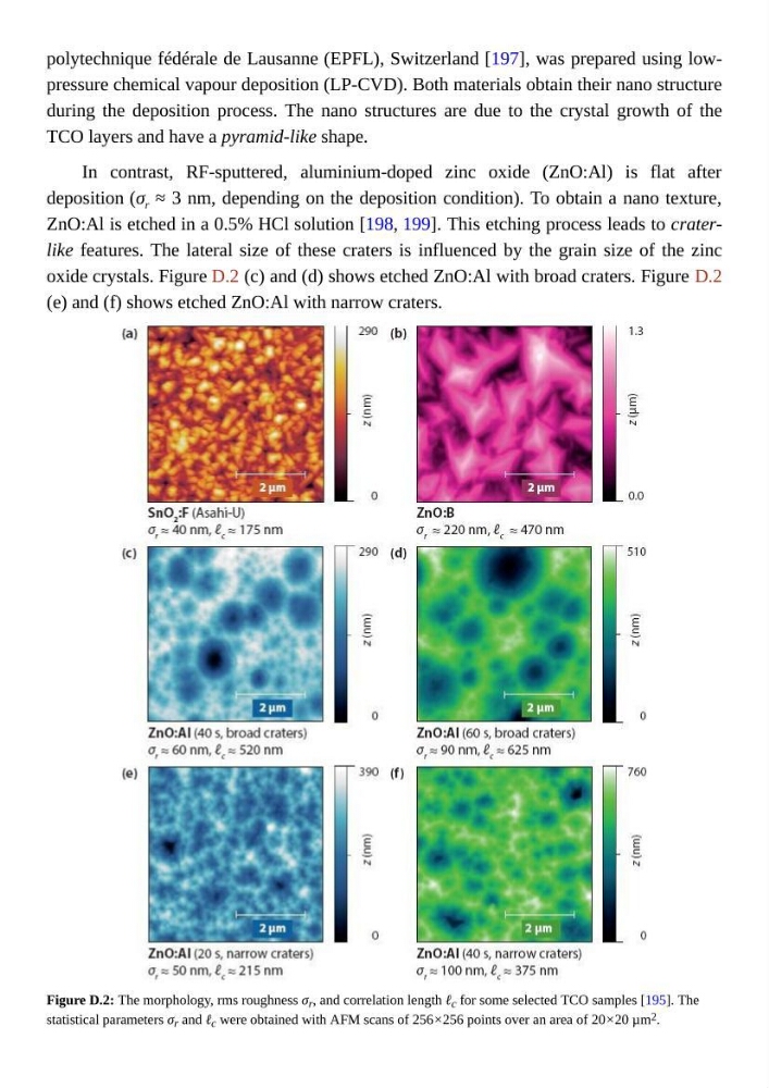
ZnO:Al is etched in a 0.5% HCl solution [198, 199]. This etching process leads to craterlike features. The lateral size of these craters is influenced by the grain size of the zinc
oxide crystals. Figure D.2 (c) and (d) shows etched ZnO:Al with broad craters. Figure D.2
(e) and (f) shows etched ZnO:Al with narrow craters.
Figure D.2: The morphology, rms roughness σ r , and correlation length ℓ c for some selected TCO samples [195]. The
statistical parameters σ r and ℓ c were obtained with AFM scans of 256×256 points over an area of 20×20 µm 2 .
during the deposition process. The nano structures are due to the crystal growth of the
TCO layers and have a pyramid-like shape.
In contrast, RF-sputtered, aluminium-doped zinc oxide (ZnO:Al) is flat after
deposition (σ r ≈ 3 nm, depending on the deposition condition). To obtain a nano texture,
ZnO:Al is etched in a 0.5% HCl solution [198, 199]. This etching process leads to craterlike features. The lateral size of these craters is influenced by the grain size of the zinc
oxide crystals. Figure D.2 (c) and (d) shows etched ZnO:Al with broad craters. Figure D.2
(e) and (f) shows etched ZnO:Al with narrow craters.
Figure D.2: The morphology, rms roughness σ r , and correlation length ℓ c for some selected TCO samples [195]. The
statistical parameters σ r and ℓ c were obtained with AFM scans of 256×256 points over an area of 20×20 µm 2 .