

14.4
14.4.1
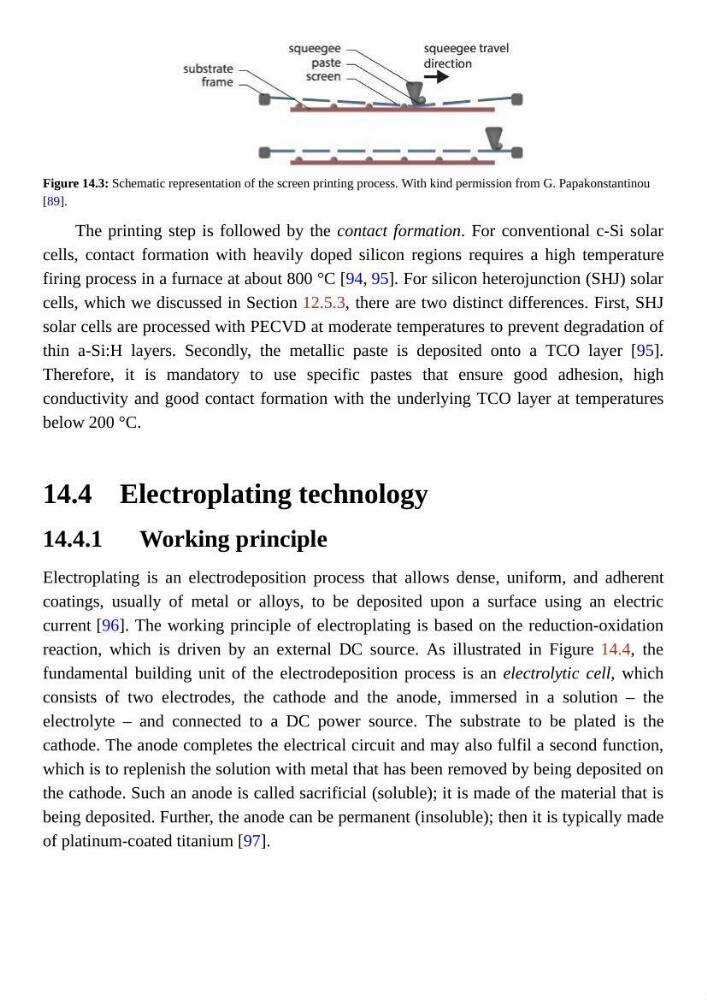
Figure 14.3: Schematic representation of the screen printing process. With kind permission from G. Papakonstantinou
[89].
The printing step is followed by the contact formation. For conventional c-Si solar
cells, contact formation with heavily doped silicon regions requires a high temperature
firing process in a furnace at about 800 °C [94, 95]. For silicon heterojunction (SHJ) solar
cells, which we discussed in Section 12.5.3, there are two distinct differences. First, SHJ
solar cells are processed with PECVD at moderate temperatures to prevent degradation of
thin a-Si:H layers. Secondly, the metallic paste is deposited onto a TCO layer [95].
Therefore, it is mandatory to use specific pastes that ensure good adhesion, high
conductivity and good contact formation with the underlying TCO layer at temperatures
below 200 °C.
Electroplating technology
Working principle
Electroplating is an electrodeposition process that allows dense, uniform, and adherent
coatings, usually of metal or alloys, to be deposited upon a surface using an electric
current [96]. The working principle of electroplating is based on the reduction-oxidation
reaction, which is driven by an external DC source. As illustrated in Figure 14.4, the
fundamental building unit of the electrodeposition process is an electrolytic cell, which
consists of two electrodes, the cathode and the anode, immersed in a solution – the
electrolyte – and connected to a DC power source. The substrate to be plated is the
cathode. The anode completes the electrical circuit and may also fulfil a second function,
which is to replenish the solution with metal that has been removed by being deposited on
the cathode. Such an anode is called sacrificial (soluble); it is made of the material that is
being deposited. Further, the anode can be permanent (insoluble); then it is typically made
of platinum-coated titanium [97].
14.4.1
Figure 14.3: Schematic representation of the screen printing process. With kind permission from G. Papakonstantinou
[89].
The printing step is followed by the contact formation. For conventional c-Si solar
cells, contact formation with heavily doped silicon regions requires a high temperature
firing process in a furnace at about 800 °C [94, 95]. For silicon heterojunction (SHJ) solar
cells, which we discussed in Section 12.5.3, there are two distinct differences. First, SHJ
solar cells are processed with PECVD at moderate temperatures to prevent degradation of
thin a-Si:H layers. Secondly, the metallic paste is deposited onto a TCO layer [95].
Therefore, it is mandatory to use specific pastes that ensure good adhesion, high
conductivity and good contact formation with the underlying TCO layer at temperatures
below 200 °C.
Electroplating technology
Working principle
Electroplating is an electrodeposition process that allows dense, uniform, and adherent
coatings, usually of metal or alloys, to be deposited upon a surface using an electric
current [96]. The working principle of electroplating is based on the reduction-oxidation
reaction, which is driven by an external DC source. As illustrated in Figure 14.4, the
fundamental building unit of the electrodeposition process is an electrolytic cell, which
consists of two electrodes, the cathode and the anode, immersed in a solution – the
electrolyte – and connected to a DC power source. The substrate to be plated is the
cathode. The anode completes the electrical circuit and may also fulfil a second function,
which is to replenish the solution with metal that has been removed by being deposited on
the cathode. Such an anode is called sacrificial (soluble); it is made of the material that is
being deposited. Further, the anode can be permanent (insoluble); then it is typically made
of platinum-coated titanium [97].