

14.2.2
Sputtering is a common physical vapour deposition (PVD) method, where energy and
momentum from an accelerated atom or ion are transmitted to atoms on a target via
sequential collisions. Consequently, these atoms can escape from the target and shift to the
gas phase, hence evaporate. Sputtering can be accomplished with two different power
supply configurations that employ magnetrons, reactive direct current (DC) and radio
frequency (RF). DC sputtering is restricted to conducting materials, whereas RF sputtering
may be also used for dielectrics.
Figure 14.1 (b) illustrates the process of sputtering. The sputtering material is
deposited onto the substrate (anode) by bombarding the target (cathode) with ions. The
vacuum chamber is kept under a well-defined pressure with inert argon gas (Ar), such that
an argon plasma can be inflamed by an oscillating electromagnetic field between the
anode and the cathode. This process generates and accelerates positively-charged argon
ions (Ar
+
) that bombard the target surface. Due to this bombardment, atoms are ejected
from the target and can form a layer on the substrate. In addition to the Ar, other gases like
nitrogen (N) can be used in order to produce nitridic coatings.
Sputtering can be used to deposit transparent conducting oxide layers such as indium
tin oxide or aluminium-doped zinc oxide. While for the former a target consisting of ZnO
and 2% Al is used, for the latter the target consists of 10% SnO 2 and 90% In 2 O 3 . However,
sputtering can also be used for depositing metallic layers that are used as electrical front
and/or back contacts.
Evaporation
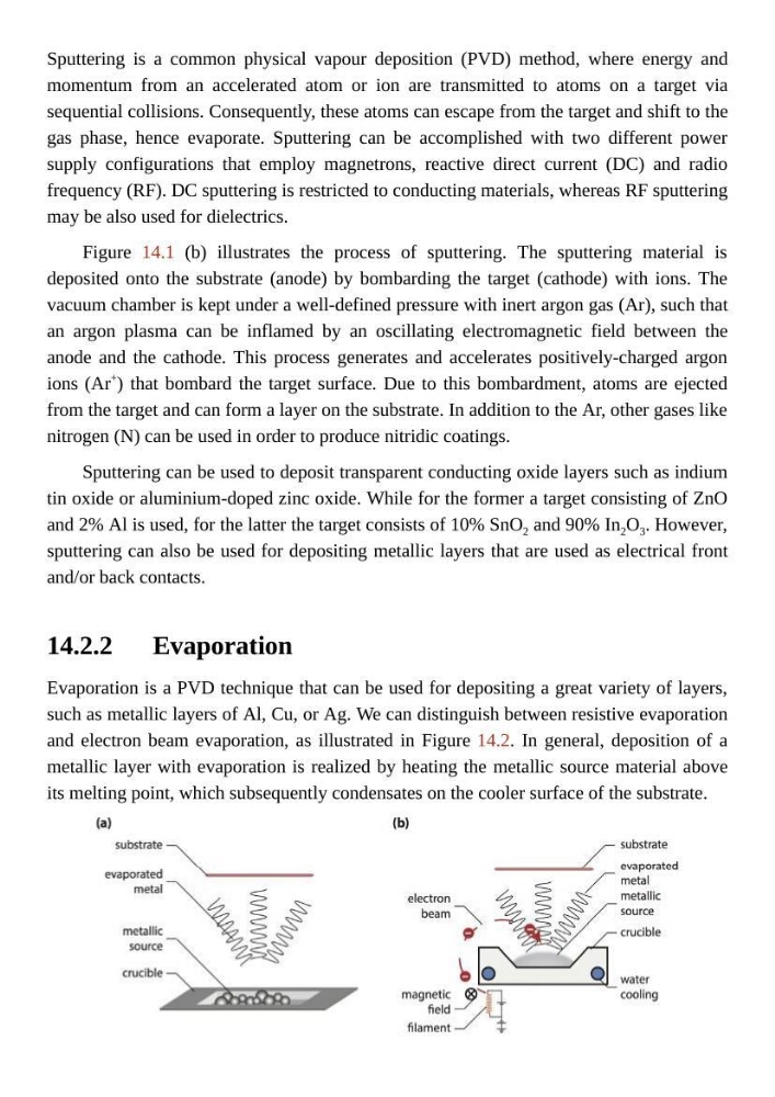
Evaporation is a PVD technique that can be used for depositing a great variety of layers,
such as metallic layers of Al, Cu, or Ag. We can distinguish between resistive evaporation
and electron beam evaporation, as illustrated in Figure 14.2. In general, deposition of a
metallic layer with evaporation is realized by heating the metallic source material above
its melting point, which subsequently condensates on the cooler surface of the substrate.
Sputtering is a common physical vapour deposition (PVD) method, where energy and
momentum from an accelerated atom or ion are transmitted to atoms on a target via
sequential collisions. Consequently, these atoms can escape from the target and shift to the
gas phase, hence evaporate. Sputtering can be accomplished with two different power
supply configurations that employ magnetrons, reactive direct current (DC) and radio
frequency (RF). DC sputtering is restricted to conducting materials, whereas RF sputtering
may be also used for dielectrics.
Figure 14.1 (b) illustrates the process of sputtering. The sputtering material is
deposited onto the substrate (anode) by bombarding the target (cathode) with ions. The
vacuum chamber is kept under a well-defined pressure with inert argon gas (Ar), such that
an argon plasma can be inflamed by an oscillating electromagnetic field between the
anode and the cathode. This process generates and accelerates positively-charged argon
ions (Ar
+
) that bombard the target surface. Due to this bombardment, atoms are ejected
from the target and can form a layer on the substrate. In addition to the Ar, other gases like
nitrogen (N) can be used in order to produce nitridic coatings.
Sputtering can be used to deposit transparent conducting oxide layers such as indium
tin oxide or aluminium-doped zinc oxide. While for the former a target consisting of ZnO
and 2% Al is used, for the latter the target consists of 10% SnO 2 and 90% In 2 O 3 . However,
sputtering can also be used for depositing metallic layers that are used as electrical front
and/or back contacts.
Evaporation
Evaporation is a PVD technique that can be used for depositing a great variety of layers,
such as metallic layers of Al, Cu, or Ag. We can distinguish between resistive evaporation
and electron beam evaporation, as illustrated in Figure 14.2. In general, deposition of a
metallic layer with evaporation is realized by heating the metallic source material above
its melting point, which subsequently condensates on the cooler surface of the substrate.