

the Se:S ratio y, the bandgap of CIGS can be tuned from 1.0 eV to 1.7 eV. As CIGS(S) is a
direct bandgap semiconductor material, it has a large absorption coefficient, hence an
absorber thickness of 1–2 μm is sufficient to absorb a large fraction of the light with
energies above the bandgap energy. Also the typical electron diffusion length is in the
order of a few micrometers. CIGS(S) is a p-type semiconductor, the p-type character
resulting from intrinsic defects in the material that among others are related to Cu
deficiencies. The many different types of defects in CIGS(S) and their properties are a
topic of ongoing research.
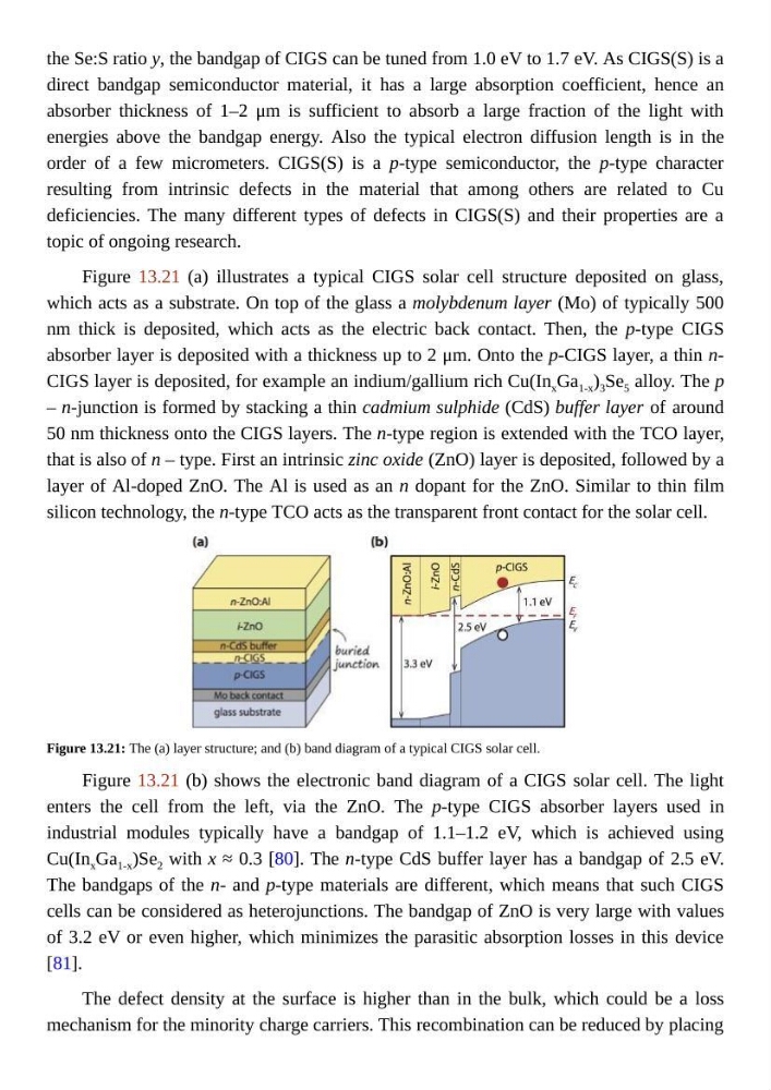
Figure 13.21 (a) illustrates a typical CIGS solar cell structure deposited on glass,
which acts as a substrate. On top of the glass a molybdenum layer (Mo) of typically 500
nm thick is deposited, which acts as the electric back contact. Then, the p-type CIGS
absorber layer is deposited with a thickness up to 2 μm. Onto the p-CIGS layer, a thin nCIGS layer is deposited, for example an indium/gallium rich Cu(In x Ga 1-x ) 3 Se 5 alloy. The p
– n-junction is formed by stacking a thin cadmium sulphide (CdS) buffer layer of around
50 nm thickness onto the CIGS layers. The n-type region is extended with the TCO layer,
that is also of n – type. First an intrinsic zinc oxide (ZnO) layer is deposited, followed by a
layer of Al-doped ZnO. The Al is used as an n dopant for the ZnO. Similar to thin film
silicon technology, the n-type TCO acts as the transparent front contact for the solar cell.
Figure 13.21: The (a) layer structure; and (b) band diagram of a typical CIGS solar cell.
Figure 13.21 (b) shows the electronic band diagram of a CIGS solar cell. The light
enters the cell from the left, via the ZnO. The p-type CIGS absorber layers used in
industrial modules typically have a bandgap of 1.1–1.2 eV, which is achieved using
Cu(In x Ga 1-x )Se 2 with x ≈ 0.3 [80]. The n-type CdS buffer layer has a bandgap of 2.5 eV.
The bandgaps of the n- and p-type materials are different, which means that such CIGS
cells can be considered as heterojunctions. The bandgap of ZnO is very large with values
of 3.2 eV or even higher, which minimizes the parasitic absorption losses in this device
[81].
The defect density at the surface is higher than in the bulk, which could be a loss
mechanism for the minority charge carriers. This recombination can be reduced by placing
direct bandgap semiconductor material, it has a large absorption coefficient, hence an
absorber thickness of 1–2 μm is sufficient to absorb a large fraction of the light with
energies above the bandgap energy. Also the typical electron diffusion length is in the
order of a few micrometers. CIGS(S) is a p-type semiconductor, the p-type character
resulting from intrinsic defects in the material that among others are related to Cu
deficiencies. The many different types of defects in CIGS(S) and their properties are a
topic of ongoing research.
Figure 13.21 (a) illustrates a typical CIGS solar cell structure deposited on glass,
which acts as a substrate. On top of the glass a molybdenum layer (Mo) of typically 500
nm thick is deposited, which acts as the electric back contact. Then, the p-type CIGS
absorber layer is deposited with a thickness up to 2 μm. Onto the p-CIGS layer, a thin nCIGS layer is deposited, for example an indium/gallium rich Cu(In x Ga 1-x ) 3 Se 5 alloy. The p
– n-junction is formed by stacking a thin cadmium sulphide (CdS) buffer layer of around
50 nm thickness onto the CIGS layers. The n-type region is extended with the TCO layer,
that is also of n – type. First an intrinsic zinc oxide (ZnO) layer is deposited, followed by a
layer of Al-doped ZnO. The Al is used as an n dopant for the ZnO. Similar to thin film
silicon technology, the n-type TCO acts as the transparent front contact for the solar cell.
Figure 13.21: The (a) layer structure; and (b) band diagram of a typical CIGS solar cell.
Figure 13.21 (b) shows the electronic band diagram of a CIGS solar cell. The light
enters the cell from the left, via the ZnO. The p-type CIGS absorber layers used in
industrial modules typically have a bandgap of 1.1–1.2 eV, which is achieved using
Cu(In x Ga 1-x )Se 2 with x ≈ 0.3 [80]. The n-type CdS buffer layer has a bandgap of 2.5 eV.
The bandgaps of the n- and p-type materials are different, which means that such CIGS
cells can be considered as heterojunctions. The bandgap of ZnO is very large with values
of 3.2 eV or even higher, which minimizes the parasitic absorption losses in this device
[81].
The defect density at the surface is higher than in the bulk, which could be a loss
mechanism for the minority charge carriers. This recombination can be reduced by placing