

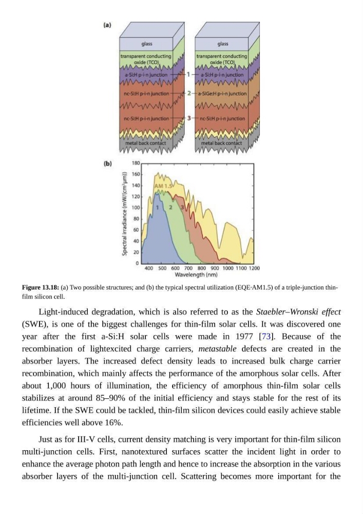
Figure 13.18: (a) Two possible structures; and (b) the typical spectral utilization (EQE·AM1.5) of a triple-junction thinfilm silicon cell.
Light-induced degradation, which is also referred to as the Staebler–Wronski effect
(SWE), is one of the biggest challenges for thin-film solar cells. It was discovered one
year after the first a-Si:H solar cells were made in 1977 [73]. Because of the
recombination of lightexcited charge carriers, metastable defects are created in the
absorber layers. The increased defect density leads to increased bulk charge carrier
recombination, which mainly affects the performance of the amorphous solar cells. After
about 1,000 hours of illumination, the efficiency of amorphous thin-film solar cells
stabilizes at around 85–90% of the initial efficiency and stays stable for the rest of its
lifetime. If the SWE could be tackled, thin-film silicon devices could easily achieve stable
efficiencies well above 16%.
Just as for III-V cells, current density matching is very important for thin-film silicon
multi-junction cells. First, nanotextured surfaces scatter the incident light in order to
enhance the average photon path length and hence to increase the absorption in the various
absorber layers of the multi-junction cell. Scattering becomes more important for the
Light-induced degradation, which is also referred to as the Staebler–Wronski effect
(SWE), is one of the biggest challenges for thin-film solar cells. It was discovered one
year after the first a-Si:H solar cells were made in 1977 [73]. Because of the
recombination of lightexcited charge carriers, metastable defects are created in the
absorber layers. The increased defect density leads to increased bulk charge carrier
recombination, which mainly affects the performance of the amorphous solar cells. After
about 1,000 hours of illumination, the efficiency of amorphous thin-film solar cells
stabilizes at around 85–90% of the initial efficiency and stays stable for the rest of its
lifetime. If the SWE could be tackled, thin-film silicon devices could easily achieve stable
efficiencies well above 16%.
Just as for III-V cells, current density matching is very important for thin-film silicon
multi-junction cells. First, nanotextured surfaces scatter the incident light in order to
enhance the average photon path length and hence to increase the absorption in the various
absorber layers of the multi-junction cell. Scattering becomes more important for the