

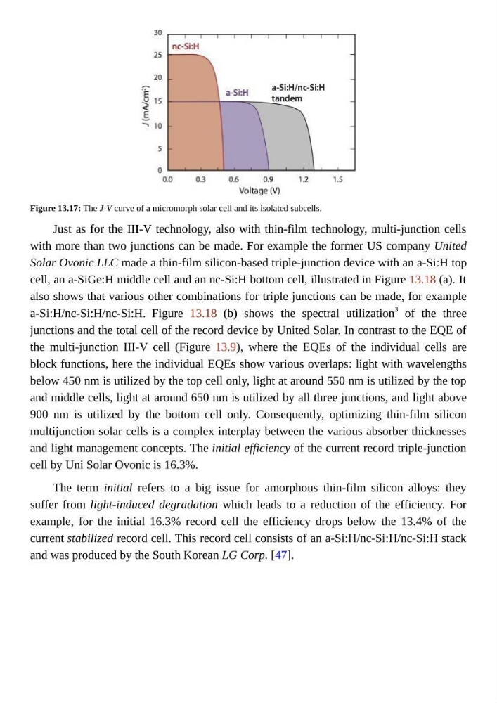
Figure 13.17: The J-V curve of a micromorph solar cell and its isolated subcells.
Just as for the III-V technology, also with thin-film technology, multi-junction cells
with more than two junctions can be made. For example the former US company United
Solar Ovonic LLC made a thin-film silicon-based triple-junction device with an a-Si:H top
cell, an a-SiGe:H middle cell and an nc-Si:H bottom cell, illustrated in Figure 13.18 (a). It
also shows that various other combinations for triple junctions can be made, for example
a-Si:H/nc-Si:H/nc-Si:H. Figure 13.18 (b) shows the spectral utilization
3 of the three
junctions and the total cell of the record device by United Solar. In contrast to the EQE of
the multi-junction III-V cell (Figure 13.9), where the EQEs of the individual cells are
block functions, here the individual EQEs show various overlaps: light with wavelengths
below 450 nm is utilized by the top cell only, light at around 550 nm is utilized by the top
and middle cells, light at around 650 nm is utilized by all three junctions, and light above
900 nm is utilized by the bottom cell only. Consequently, optimizing thin-film silicon
multijunction solar cells is a complex interplay between the various absorber thicknesses
and light management concepts. The initial efficiency of the current record triple-junction
cell by Uni Solar Ovonic is 16.3%.
The term initial refers to a big issue for amorphous thin-film silicon alloys: they
suffer from light-induced degradation which leads to a reduction of the efficiency. For
example, for the initial 16.3% record cell the efficiency drops below the 13.4% of the
current stabilized record cell. This record cell consists of an a-Si:H/nc-Si:H/nc-Si:H stack
and was produced by the South Korean LG Corp. [47].
Just as for the III-V technology, also with thin-film technology, multi-junction cells
with more than two junctions can be made. For example the former US company United
Solar Ovonic LLC made a thin-film silicon-based triple-junction device with an a-Si:H top
cell, an a-SiGe:H middle cell and an nc-Si:H bottom cell, illustrated in Figure 13.18 (a). It
also shows that various other combinations for triple junctions can be made, for example
a-Si:H/nc-Si:H/nc-Si:H. Figure 13.18 (b) shows the spectral utilization
3 of the three
junctions and the total cell of the record device by United Solar. In contrast to the EQE of
the multi-junction III-V cell (Figure 13.9), where the EQEs of the individual cells are
block functions, here the individual EQEs show various overlaps: light with wavelengths
below 450 nm is utilized by the top cell only, light at around 550 nm is utilized by the top
and middle cells, light at around 650 nm is utilized by all three junctions, and light above
900 nm is utilized by the bottom cell only. Consequently, optimizing thin-film silicon
multijunction solar cells is a complex interplay between the various absorber thicknesses
and light management concepts. The initial efficiency of the current record triple-junction
cell by Uni Solar Ovonic is 16.3%.
The term initial refers to a big issue for amorphous thin-film silicon alloys: they
suffer from light-induced degradation which leads to a reduction of the efficiency. For
example, for the initial 16.3% record cell the efficiency drops below the 13.4% of the
current stabilized record cell. This record cell consists of an a-Si:H/nc-Si:H/nc-Si:H stack
and was produced by the South Korean LG Corp. [47].