

For example, if we use a low bandgap material, a large fraction of the energy carried
by the photons is not used. However, if we use more bandgaps, the same amount of
photons can be used but less energy is wasted as heat. Thus, large parts of the solar
spectrum and large parts of the energy in the solar spectrum can be utilized at the same
time, if more than one p-n junctions are used.
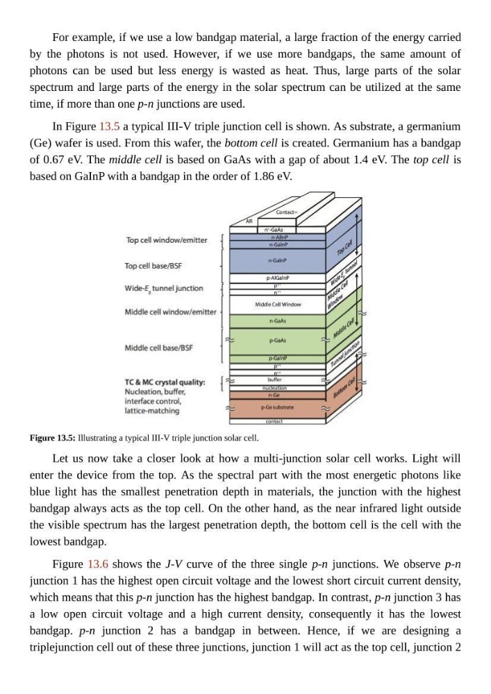
In Figure 13.5 a typical III-V triple junction cell is shown. As substrate, a germanium
(Ge) wafer is used. From this wafer, the bottom cell is created. Germanium has a bandgap
of 0.67 eV. The middle cell is based on GaAs with a gap of about 1.4 eV. The top cell is
based on GaInP with a bandgap in the order of 1.86 eV.
Figure 13.5: Illustrating a typical III-V triple junction solar cell.
Let us now take a closer look at how a multi-junction solar cell works. Light will
enter the device from the top. As the spectral part with the most energetic photons like
blue light has the smallest penetration depth in materials, the junction with the highest
bandgap always acts as the top cell. On the other hand, as the near infrared light outside
the visible spectrum has the largest penetration depth, the bottom cell is the cell with the
lowest bandgap.
Figure 13.6 shows the J-V curve of the three single p-n junctions. We observe p-n
junction 1 has the highest open circuit voltage and the lowest short circuit current density,
which means that this p-n junction has the highest bandgap. In contrast, p-n junction 3 has
a low open circuit voltage and a high current density, consequently it has the lowest
bandgap. p-n junction 2 has a bandgap in between. Hence, if we are designing a
triplejunction cell out of these three junctions, junction 1 will act as the top cell, junction 2
by the photons is not used. However, if we use more bandgaps, the same amount of
photons can be used but less energy is wasted as heat. Thus, large parts of the solar
spectrum and large parts of the energy in the solar spectrum can be utilized at the same
time, if more than one p-n junctions are used.
In Figure 13.5 a typical III-V triple junction cell is shown. As substrate, a germanium
(Ge) wafer is used. From this wafer, the bottom cell is created. Germanium has a bandgap
of 0.67 eV. The middle cell is based on GaAs with a gap of about 1.4 eV. The top cell is
based on GaInP with a bandgap in the order of 1.86 eV.
Figure 13.5: Illustrating a typical III-V triple junction solar cell.
Let us now take a closer look at how a multi-junction solar cell works. Light will
enter the device from the top. As the spectral part with the most energetic photons like
blue light has the smallest penetration depth in materials, the junction with the highest
bandgap always acts as the top cell. On the other hand, as the near infrared light outside
the visible spectrum has the largest penetration depth, the bottom cell is the cell with the
lowest bandgap.
Figure 13.6 shows the J-V curve of the three single p-n junctions. We observe p-n
junction 1 has the highest open circuit voltage and the lowest short circuit current density,
which means that this p-n junction has the highest bandgap. In contrast, p-n junction 3 has
a low open circuit voltage and a high current density, consequently it has the lowest
bandgap. p-n junction 2 has a bandgap in between. Hence, if we are designing a
triplejunction cell out of these three junctions, junction 1 will act as the top cell, junction 2