

13.1
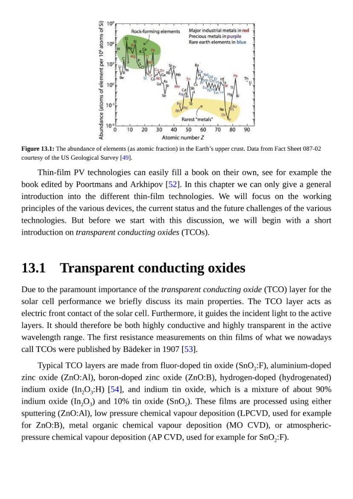
Figure 13.1: The abundance of elements (as atomic fraction) in the Earth’s upper crust. Data from Fact Sheet 087-02
courtesy of the US Geological Survey [49].
Thin-film PV technologies can easily fill a book on their own, see for example the
book edited by Poortmans and Arkhipov [52]. In this chapter we can only give a general
introduction into the different thin-film technologies. We will focus on the working
principles of the various devices, the current status and the future challenges of the various
technologies. But before we start with this discussion, we will begin with a short
introduction on transparent conducting oxides (TCOs).
Transparent conducting oxides
Due to the paramount importance of the transparent conducting oxide (TCO) layer for the
solar cell performance we briefly discuss its main properties. The TCO layer acts as
electric front contact of the solar cell. Furthermore, it guides the incident light to the active
layers. It should therefore be both highly conductive and highly transparent in the active
wavelength range. The first resistance measurements on thin films of what we nowadays
call TCOs were published by Bädeker in 1907 [53].
Typical TCO layers are made from fluor-doped tin oxide (SnO 2 :F), aluminium-doped
zinc oxide (ZnO:Al), boron-doped zinc oxide (ZnO:B), hydrogen-doped (hydrogenated)
indium oxide (In 2 O 3 :H) [54], and indium tin oxide, which is a mixture of about 90%
indium oxide (In 2 O 3 ) and 10% tin oxide (SnO 2 ). These films are processed using either
sputtering (ZnO:Al), low pressure chemical vapour deposition (LPCVD, used for example
for ZnO:B), metal organic chemical vapour deposition (MO CVD), or atmosphericpressure chemical vapour deposition (AP CVD, used for example for SnO 2 :F).
Figure 13.1: The abundance of elements (as atomic fraction) in the Earth’s upper crust. Data from Fact Sheet 087-02
courtesy of the US Geological Survey [49].
Thin-film PV technologies can easily fill a book on their own, see for example the
book edited by Poortmans and Arkhipov [52]. In this chapter we can only give a general
introduction into the different thin-film technologies. We will focus on the working
principles of the various devices, the current status and the future challenges of the various
technologies. But before we start with this discussion, we will begin with a short
introduction on transparent conducting oxides (TCOs).
Transparent conducting oxides
Due to the paramount importance of the transparent conducting oxide (TCO) layer for the
solar cell performance we briefly discuss its main properties. The TCO layer acts as
electric front contact of the solar cell. Furthermore, it guides the incident light to the active
layers. It should therefore be both highly conductive and highly transparent in the active
wavelength range. The first resistance measurements on thin films of what we nowadays
call TCOs were published by Bädeker in 1907 [53].
Typical TCO layers are made from fluor-doped tin oxide (SnO 2 :F), aluminium-doped
zinc oxide (ZnO:Al), boron-doped zinc oxide (ZnO:B), hydrogen-doped (hydrogenated)
indium oxide (In 2 O 3 :H) [54], and indium tin oxide, which is a mixture of about 90%
indium oxide (In 2 O 3 ) and 10% tin oxide (SnO 2 ). These films are processed using either
sputtering (ZnO:Al), low pressure chemical vapour deposition (LPCVD, used for example
for ZnO:B), metal organic chemical vapour deposition (MO CVD), or atmosphericpressure chemical vapour deposition (AP CVD, used for example for SnO 2 :F).