

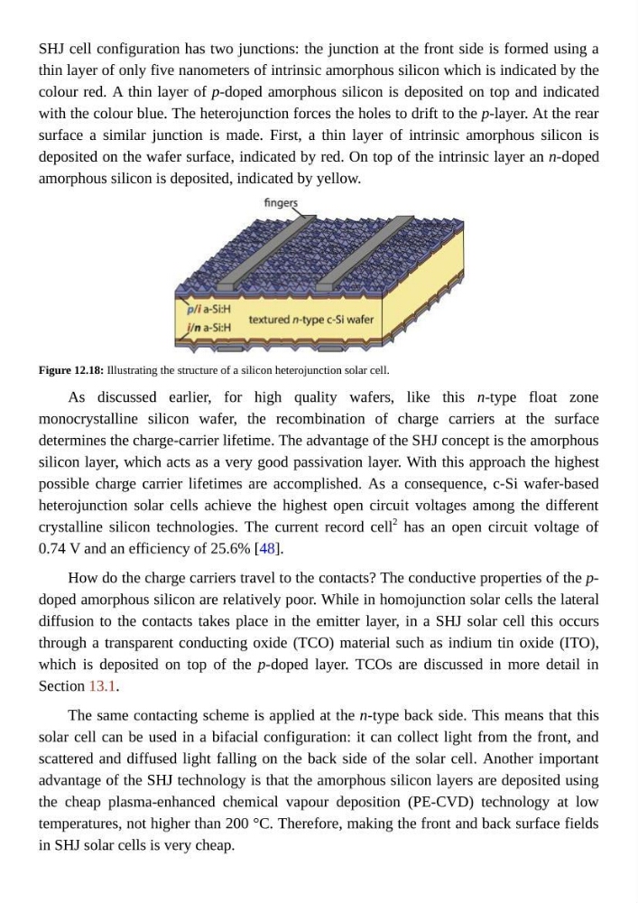
SHJ cell configuration has two junctions: the junction at the front side is formed using a
thin layer of only five nanometers of intrinsic amorphous silicon which is indicated by the
colour red. A thin layer of p-doped amorphous silicon is deposited on top and indicated
with the colour blue. The heterojunction forces the holes to drift to the p-layer. At the rear
surface a similar junction is made. First, a thin layer of intrinsic amorphous silicon is
deposited on the wafer surface, indicated by red. On top of the intrinsic layer an n-doped
amorphous silicon is deposited, indicated by yellow.
Figure 12.18: Illustrating the structure of a silicon heterojunction solar cell.
As discussed earlier, for high quality wafers, like this n-type float zone
monocrystalline silicon wafer, the recombination of charge carriers at the surface
determines the charge-carrier lifetime. The advantage of the SHJ concept is the amorphous
silicon layer, which acts as a very good passivation layer. With this approach the highest
possible charge carrier lifetimes are accomplished. As a consequence, c-Si wafer-based
heterojunction solar cells achieve the highest open circuit voltages among the different
crystalline silicon technologies. The current record cell
2
has an open circuit voltage of
0.74 V and an efficiency of 25.6% [48].
How do the charge carriers travel to the contacts? The conductive properties of the pdoped amorphous silicon are relatively poor. While in homojunction solar cells the lateral
diffusion to the contacts takes place in the emitter layer, in a SHJ solar cell this occurs
through a transparent conducting oxide (TCO) material such as indium tin oxide (ITO),
which is deposited on top of the p-doped layer. TCOs are discussed in more detail in
Section 13.1.
The same contacting scheme is applied at the n-type back side. This means that this
solar cell can be used in a bifacial configuration: it can collect light from the front, and
scattered and diffused light falling on the back side of the solar cell. Another important
advantage of the SHJ technology is that the amorphous silicon layers are deposited using
the cheap plasma-enhanced chemical vapour deposition (PE-CVD) technology at low
temperatures, not higher than 200 °C. Therefore, making the front and back surface fields
in SHJ solar cells is very cheap.
thin layer of only five nanometers of intrinsic amorphous silicon which is indicated by the
colour red. A thin layer of p-doped amorphous silicon is deposited on top and indicated
with the colour blue. The heterojunction forces the holes to drift to the p-layer. At the rear
surface a similar junction is made. First, a thin layer of intrinsic amorphous silicon is
deposited on the wafer surface, indicated by red. On top of the intrinsic layer an n-doped
amorphous silicon is deposited, indicated by yellow.
Figure 12.18: Illustrating the structure of a silicon heterojunction solar cell.
As discussed earlier, for high quality wafers, like this n-type float zone
monocrystalline silicon wafer, the recombination of charge carriers at the surface
determines the charge-carrier lifetime. The advantage of the SHJ concept is the amorphous
silicon layer, which acts as a very good passivation layer. With this approach the highest
possible charge carrier lifetimes are accomplished. As a consequence, c-Si wafer-based
heterojunction solar cells achieve the highest open circuit voltages among the different
crystalline silicon technologies. The current record cell
2
has an open circuit voltage of
0.74 V and an efficiency of 25.6% [48].
How do the charge carriers travel to the contacts? The conductive properties of the pdoped amorphous silicon are relatively poor. While in homojunction solar cells the lateral
diffusion to the contacts takes place in the emitter layer, in a SHJ solar cell this occurs
through a transparent conducting oxide (TCO) material such as indium tin oxide (ITO),
which is deposited on top of the p-doped layer. TCOs are discussed in more detail in
Section 13.1.
The same contacting scheme is applied at the n-type back side. This means that this
solar cell can be used in a bifacial configuration: it can collect light from the front, and
scattered and diffused light falling on the back side of the solar cell. Another important
advantage of the SHJ technology is that the amorphous silicon layers are deposited using
the cheap plasma-enhanced chemical vapour deposition (PE-CVD) technology at low
temperatures, not higher than 200 °C. Therefore, making the front and back surface fields
in SHJ solar cells is very cheap.